• Photonics Research
  • Vol. 10, Issue 9, 2229 (2022)
Jiabing Lu1, Zesheng Lv1, Xinjia Qiu1, Shiquan Lai1, and Hao Jiang1、2、3、*
Author Affiliations
  • 1School of Electronics and Information Technology, Sun Yat-sen University, Guangzhou 510006, China
  • 2State Key Laboratory of Optoelectronic Materials and Technologies, Sun Yat-sen University, Guangzhou 510006, China
  • 3Guangdong Engineering Technology R & D Center of Compound Semiconductors and Devices, Sun Yat-sen University, Guangzhou 510006, China
  • show less
    DOI: 10.1364/PRJ.467689 Cite this Article Set citation alerts
    Jiabing Lu, Zesheng Lv, Xinjia Qiu, Shiquan Lai, Hao Jiang. Ultrasensitive and high-speed AlGaN/AlN solar-blind ultraviolet photodetector: a full-channel-self-depleted phototransistor by a virtual photogate[J]. Photonics Research, 2022, 10(9): 2229 Copy Citation Text show less

    Abstract

    High sensitivity, high solar rejection ratio, and fast response are essential characteristics for most practical applications of solar-blind ultraviolet (UV) detectors. These features, however, usually require a complex device structure, complicated process, and high operating voltage. Herein, a simply structured n-AlGaN/AlN phototransistor with a self-depleted full channel is reported. The self-depletion of the highly conductive n-AlGaN channel is achieved by exploiting the strong polarization-induced electric field therein to act as a virtual photogate. The resulting two-terminal detectors with interdigital Ohmic electrodes exhibit an ultrahigh gain of 1.3×10⁵, an ultrafast response speed with rise/decay times of 537.5 ps/3.1 μs, and an ultrahigh Johnson and shot noise (flicker noise) limited specific detectivity of 1.5×10¹⁸ (4.7×10¹⁶) Jones at 20-V bias. Also, a very low dark current of the order of pA and a photo-to-dark current ratio of above 108 are obtained, due to the complete depletion of the n-Al0.5Ga0.5N channel layer and the high optical gain. The proposed planar phototransistor combines fabrication simplicity and performance advantages, and thus is promising in a variety of UV detection applications.

    1. INTRODUCTION

    With the exploration and development of wide bandgap semiconductors, solid-state solar-blind ultraviolet (SBUV) photodetectors have attracted more and more research attention [13]. The SBUV detection, however, sets out unique requirements for the “5S” key parameters (i.e., high sensitivity, high spectral selectivity, high signal-to-noise ratio, high speed, and high stability) of usual high-performance photodetectors. Since the SBUV signal (200–280 nm) is easily attenuated during propagation and is usually very weak, high sensitivity is particularly important for the photodetectors. Sensitivity of 1018 to 109  W/cm2 is generally required for flame or corona discharge detection [4,5]. Moreover, besides the spectral response cutoff of less than 280 nm, the out-of-band rejection ratio is expected to be higher than 108 of the current photomultiplier tube with a filter [6]. In the past decades, although research efforts have led to the realization of different types of high-sensitivity SBUV photodetectors on III nitride [710] and oxide wide bandgap semiconductors [1114], they are still far from the demand for industrial applications.

    Generally, high internal gain is a prerequisite to achieve high sensitivity of photodetectors. The main types of high-gain photodetectors are avalanche photodiodes (APDs), unipolar field-effect phototransistors (FEPTs), and bipolar heterojunction phototransistors (HPTs). Despite the multiplication gain of more than 1×10⁵ achieved in AlGaN SBUV APDs [15], the high requirements on epitaxial quality and operating voltage stability strongly constrain their development [16]. Moreover, since the pn junction is the building block of conventional APD and HPT device structures, the common problem of p-type doping in wide bandgap semiconductors is an obstacle to the fabrication of high-performance devices. The redistribution of p-type dopant in the base layer of HPTs often causes performance degradation [17]. In contrast, unipolar FEPTs are relatively simple in epitaxial structure and have the advantage of realizing on-chip micro optoelectronic systems through monolithic integration [18]. For wurtzite structure AlGaN, the two-dimensional electron gas (2DEG) generated at the undoped heterointerface due to the inherent polarization effect is more favorable to the construction of high-gain FEPT based on high electron mobility. However, the usual FEPT detectors are three-terminal devices, which require a negatively biased gate to achieve a low dark current in the off state [11]. Moreover, FEPTs also suffer from a serious persistent photoconductivity effect due to deep-level defects in the barrier or insulator layer adjacent to the channel [19,20]. The resulting problem is that the complexity of the device structure of high-gain photodetectors puts forward higher requirements for epitaxial materials and device technology, which limits the substantive progress of high-sensitivity high-speed SBUV photodetectors based on yet to mature wide bandgap semiconductors. Therefore, high performance by a simple device structure and process is crucial for SBUV photodetectors.

    The spontaneous polarization effect is an intrinsic property of a number of compound semiconductors, originating from the inversion asymmetry of the crystal structure [21]. In wurtzite AlGaN, in addition to spontaneous polarization, piezoelectric polarization due to the presence of biaxial stress also contributes significantly to macroscopic polarization [22]. The strong polarization effect induces a large electric field in heteroepitaxial nitrides, which not only has a significant impact on the device characteristics [23,24], but also opens up a way for the development of new structures for optoelectronic devices.

    In this work, an n-Al0.5Ga0.5N/AlN based SBUV phototransistor with a built-in virtual photogate is proposed to address the contradiction between structural and process simplicity and high detection performance. The strong polarization electric field in the n-Al0.5Ga0.5N channel layer is utilized to form the photogate, which can effectively deplete the electrons in the channel layer without illumination, and control the full channel carriers under illumination. A planar interdigital electrode configuration is used for the phototransistor, which has the advantages of a one-step fabrication process and easy integration. The fabricated photodetectors exhibit excellent performances including an ultrahigh detectivity of 1.5×10¹⁸ Jones due to a very low dark current (less than 2 pA) and ultrahigh internal gain (up to 1.3×10⁵), an ultrafast response speed with rise/decay times of 537.5 ps/3.1 μs, and a high photo-to-dark current ratio (PDCR) of 108. In addition, the photoresponse mechanism is also analyzed, and the corresponding model is presented, which provides a basis for optimizing this type of detector.

    2. EXPERIMENTS

    The Al0.5Ga0.5N/AlN photodetectors presented in this work were epitaxially grown on a 2-inch (5.08 cm) c-plane (0001) sapphire substrate by a low-pressure metal organic chemical vapor deposition (LP-MOCVD) method. Trimethyl-gallium (TMGa), trimethyl-aluminum (TMAl), and ammonia (NH3) were used as precursors of group-III metals and group-V nitrogen, while silane (SiH4) was used as an n-type doping source. A 500-nm-thick AlN was first grown on the substrate at 1080°C, and then a Si-doped n-type Al0.5Ga0.5N was deposited as an absorption and channel layer. For the epitaxial growth, n-type Al0.5Ga0.5N layers with different thicknesses were grown, in which representative structural samples of a fully depleted 70-nm-thin layer and a non-depleted 100-nm-thick layer were used to show the results. The electron concentration and mobility in the n-Al0.5Ga0.5N layers, based on the Hall-effect measurement of a 400-nm-thick n-Al0.5Ga0.5N sample, are about 1.8×10¹⁸  cm3 and 25.8  cm2/(V·s), respectively.

    After the epitaxial growth, interdigital electrodes with Ti/Al/Ni/Au (15/80/20/60 nm) metal stacks were deposited by electron-beam evaporation and thermally annealed in pure N2 atmosphere at 830°C for 30 s to form an Ohmic contact. The device area is 50  μm×99  μm, in which the number, length, width, and spacing of the electrode fingers are 13, 45 μm, 3 μm, and 5 μm, respectively. A schematic diagram of the photodetector is shown in Fig. 1.

    Schematic diagram of Al0.5Ga0.5N/AlN solar-blind UV photodetector, including (a) plan-view of interdigitated electrodes and (b) cross-sectional view, illustrates the separation of electron–hole pair generated by incident UV signal under the action of polarization electric field in the self-depleted Al0.5Ga0.5N layer.

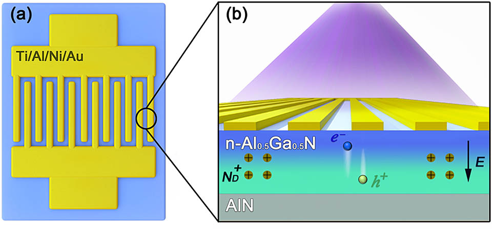
    Figure 1.Schematic diagram of Al0.5Ga0.5N/AlN solar-blind UV photodetector, including (a) plan-view of interdigitated electrodes and (b) cross-sectional view, illustrates the separation of electron–hole pair generated by incident UV signal under the action of polarization electric field in the self-depleted Al0.5Ga0.5N layer.

    The structural properties of the epitaxial samples were characterized by high-resolution X-ray diffraction (HR-XRD) measurements (Brucker D8 Discovery). The transmittance spectrum in the wavelength range of 200–800 nm was measured using a UV-visible spectrophotometer (Shimadzu UV2550). A Kelvin probe force microscope (KPFM) (Brucker Dimension Edge) was used to determine the surface potential of n-Al0.5Ga0.5N. The current–voltage (I–V) characteristics under dark and deep UV (DUV) irradiation conditions were measured using a semiconductor parameter analyzer (Keithley 4200-SCS), in which a DUV light emitting diode (LED) with a peak wavelength of 260 nm was used as the light source. Additionally, the photocurrent at different incident light powers was measured using the 260-nm LED and a 255-nm DUV lamp as irradiation sources. Noise power spectral density was collected by a multifunctional semiconductor parameter tester (PDA FS-Pro). The photoresponse measurements were conducted using a test system equipped with a deuterium lamp and bromine tungsten lamp, 1200 g/mm grating monochromator, and Newport optical power meter. The transient responses of the photodetectors were measured using a 213-nm DUV laser (Brolight MCC-213-1004) with a pulse width of 700 ps and a repetition rate of 1 kHz as the excitation source. The impulse responses were recorded by a high-speed oscilloscope (Keysight DSOS604A). All measurements were carried out at room temperature.

    3. RESULTS AND DISCUSSION

    First, the structural and optical properties of the epitaxial structure with a 70-nm-thick Al0.5Ga0.5N layer were characterized. Figure 2(a) shows the XRD rocking curves of the symmetric (0002) and asymmetric (101¯5) reflections. The full width at half maximum (FWHM) values of the (0002) rocking curves of AlN and Al0.5Ga0.5N layers are 70 and 330 arcsec, respectively, and the FWHM values of the corresponding (101¯5) rocking curves are 248 and 644 arcsec, respectively, indicating that the epitaxial sample has high crystalline quality with relatively low density dislocations. Figure 2(b) exhibits the optical transmittance spectrum of the epitaxial sample. A sharp absorption edge was found at 260  nm. The average transmittance is higher than 90% at wavelengths above 285 nm. The optical energy gap (Eg) was also determined. It can be obtained from the spectral absorption coefficient (α) derived from the transmission spectrum by using Tauc’s law: αhv=A(hvEg)n, where A is a constant, and n=1/2 for direct transitions. As shown in the inset of Fig. 2(b), the resulting Eg value of the n-Al0.5Ga0.5N layer is 4.68 eV, consistent with the bandgap value of AlGaN with Al composition of 50% [25].

    (a) (0002) plane and (101¯5) plane ω-scan curves of the epitaxial sample with the 70-nm-thick n-Al0.5Ga0.5N layer. (b) Transmission spectrum of the epitaxial sample. The inset shows the spectrum. Surface potential maps of (c) 70-nm and (d) 100-nm n-Al0.5Ga0.5N channel layers measured on 5 μm×5 μm area by KFAM using Pt-Ir tip. The map consists of 256×256 pixels, and thus each pixel represents a square with a side length about 20 nm.

    Figure 2.(a) (0002) plane and (101¯5) plane ω-scan curves of the epitaxial sample with the 70-nm-thick n-Al0.5Ga0.5N layer. (b) Transmission spectrum of the epitaxial sample. The inset shows the spectrum. Surface potential maps of (c) 70-nm and (d) 100-nm n-Al0.5Ga0.5N channel layers measured on 5  μm×5  μm area by KFAM using Pt-Ir tip. The map consists of 256×256 pixels, and thus each pixel represents a square with a side length about 20 nm.

    Second, to compare the depletion effect of the polarization electric field on the electrons in n-type Al0.5Ga0.5N channel layers with the two thicknesses, the surface potential of the channel layers was measured by KPFM. This method directly measures the contact potential difference (CPD) between the probe tip and the semiconductor surface [26]. The work function of the semiconductor can then be calculated relative to the work function of the probe tip. As represented in Figs. 2(c) and 2(d), the average CPD value of 5  μm×5  μm area calculated using Nanoscope Analysis software is 302 mV and 77 mV for the 70-nm and 100-nm channel layers, respectively. Since the electron affinity of the n-Al0.5Ga0.5N layer remains unchanged, the change of the difference between the conduction band minimum (EC) and the Fermi level (EF) at the surface will be reflected by the same change of CPD. The larger CPD value of the 70-nm channel layer sample, therefore, indicates the larger surface band bending (i.e., there is a large polarization electric field that leads to the depletion of the channel layer).

    Figures 3(a) and 3(b) show the I–V characteristics of the photodetectors under dark and irradiation conditions. The dark current (Idark) and photocurrent (Iph) of detectors present near symmetry under positive and negative applied bias. Compared with the device with a 100-nm-thick channel layer, the Idark of the 70-nm-thick channel detector is six orders of magnitude lower, meaning that the high electron concentration in the n-type Al0.5Ga0.5N channel is fully depleted by the virtual photogate introduced by the polarization electric field. As shown in Fig. 3(a), the Idark is less than 1 pA below 10-V bias and only 1.7 pA at 20-V bias. Under 260-nm radiation with an intensity of 138  μW/cm2, the Iph rapidly increased to 4.0×10⁵  A with the increase of bias voltage to 5 V and reached 1.8×10⁴  A at 20 V. Thus, a high PDCR of up to 108 magnitudes was obtained in the bias range of 10 to 20 V. In contrast, the detector with a 100-nm channel layer shows not only the much larger Idark (1.3×10⁵  A at 20 V), but also a higher Iph (1.3×10³  A at 20 V), as shown in Fig. 3(b). The higher Iph is attributed to the fact that the thicker channel layer can provide higher conductance (due to the partial depletion) and more photogenerated carriers under the DUV illumination, leading to the enhancement of the photogating (PG) effect mentioned later. This structure with a partially depleted channel, however, results in a significant degradation in PDCR (102 at 138  μW/cm2), thus affecting the detection of weak DUV signal. Furthermore, the noise power spectral density (SN) of the two device samples was measured at different bias voltages of 10, 15, and 20 V in the frequency range of 1 Hz to 100 kHz. As shown in Fig. 3(d), flicker (1/f) noise is the dominant noise mechanism in our detectors. It can also be seen that the SN of the detector with the 70-nm-thick channel layer (in green) is submerged by background noise (in black), indicating that the measured SN is overestimated because it is below the measurement limit of the instrument. However, the SN is still more than six orders of magnitude lower than the counterpart of the 100-nm-thick channel detector. For the above reasons, in the following, only the characteristics of a full-channel-self-depleted (FCSD) phototransistor with the 70-nm-thick channel are further analyzed and discussed.

    Dark and illuminated I–V curves of the n-Al0.5Ga0.5N/AlN photodetectors with (a) 70-nm channel layer and (b) 100-nm channel layer. (c) Gain characteristics and (d) noise power spectral density of the corresponding two device samples.

    Figure 3.Dark and illuminated I–V curves of the n-Al0.5Ga0.5N/AlN photodetectors with (a) 70-nm channel layer and (b) 100-nm channel layer. (c) Gain characteristics and (d) noise power spectral density of the corresponding two device samples.

    As a key parameter for high-sensitivity photodetectors, optical gain (G) was then evaluated. The gain G is defined as the ratio of photocarriers to photon flux [27], which is G=IphhvηextqPin,where hv is the incident photon energy, ηext the external quantum efficiency, q the electronic charge, and Pin the input optical power. Using a conservative estimate, ηext was assumed to be 100%, from which the calculated optical gain of the FCSD phototransistor at 20 V was 1.3×10⁵.

    Next, the photoresponse characteristics of the FCSD phototransistor were further investigated. Figure 4(a) shows the spectral responses of the detector at different bias voltages. A sharp cutoff can be found at the wavelength of 260  nm, which exactly corresponds to the band-edge absorption of the n-Al0.5Ga0.5N channel layer [Fig. 2(b)]. The out-of-band response may be caused by the defect to band transition in the depleted n-Al0.5Ga0.5N channel layer, in which the defect associated photogenerated carriers contribute to the measured Iph under the same gain mechanism. However, under all measurement bias voltages, the spectral rejection ratio of 240 to 280 nm (R240/280nm) is above the order of 102 [Fig. 4(b)], indicating the capability of true SBUV photodetection of the phototransistor. An increase of the above bandgap responsivity is shown with the increasing bias, due to the enhancement of photogenerated carrier separation at high bias and thus the increased Iph. The peak responsivity is as high as 1.6×10⁵  A/W at 240 nm and 20-V bias, as determined by R=(IphIdark)/APin, where A is the effective illumination area. In the calculation, the values of Iph, Idark, A, and Pin used are 1.6×10⁶  A, 1.7×10¹²  A, 4950  μm2, and 0.2  μW/cm2, respectively. Moreover, the responsivity remains high even at wavelengths as short as 200 nm (1.7×10⁴  A/W). It is known that the shorter the wavelength, the shallower the penetration depth. On account of this effect, the above bandgap responsivity of the phototransistor, especially HPT, usually decreases significantly with the decrease of wavelength. We attribute the relatively high responsivity at short wavelengths to the auxiliary separation of photogenerated carriers by the polarization field in the channel layer, allowing the photoholes generated near the surface to drift towards the AlGaN/AlN interface and increase the Iph due to the reduction of carrier recombination.

    Photoresponse characteristics of the FCSD phototransistor. (a) Spectral responses at different bias voltages. (b) Bias dependence of responsivity at 240 and 280 nm. (c) Time and irradiation intensity dependence of the response current under 5-V bias, in which the irradiation uses periodic DUV illumination with periodic on/off times of 10/20 s. (d) Transient responses to the 213-nm pulse signal with an optical power density of 127.3 mW/cm2 at 20-V bias. The inset shows an enlarged view of a single impulse response.

    Figure 4.Photoresponse characteristics of the FCSD phototransistor. (a) Spectral responses at different bias voltages. (b) Bias dependence of responsivity at 240 and 280 nm. (c) Time and irradiation intensity dependence of the response current under 5-V bias, in which the irradiation uses periodic DUV illumination with periodic on/off times of 10/20 s. (d) Transient responses to the 213-nm pulse signal with an optical power density of 127.3  mW/cm2 at 20-V bias. The inset shows an enlarged view of a single impulse response.

    Figure 4(c) gives the time and irradiation intensity dependence of the response current under 5 V bias. One can see that the detector clearly recognizes 260-nm periodic irradiation of different intensities with excellent stability and reproducibility. A steep rise and fall of the response current can be observed with the on and off of DUV illumination. Furthermore, the transient response of the device was measured. The load resistor used in the measurement is 50 Ω. Figure 4(d) shows the impulse responses at 20-V bias. The rise time from 10% to 90% of the response peak is 537.5 ps, while the decay time from 90% to 10% is 3.1 μs. The FWHM of a single impulse response is 130 ns, which is one of the highest response speeds of various SBUV detectors reported so far. Our calculations show that the rise time is approximate to the electron transit time (480  ps) across the 5-μm electrode spacing at 20-V bias. As the power density of the pulsed light signal decreases from 127.3 to 11.6  mW/cm2, the rise time increases from 537.5 to 662.1 ps. The reason for the slight increase in rise time may be that under the lower power density incident light, the proportion of photogenerated carriers in the inner region increases, and it takes longer for them to reach the electrodes than in the surface region. Compared to the rise time, the decay time is relatively large, which can be attributed to the fact that the recombination time of minority carriers (hole lifetime) that determines the decay of response current is prolonged by the hole drifting towards the Al0.5Ga0.5N/AlN interface under the virtual photogate. In addition, the detrapping of photogenerated carriers trapped by deep-level defects may also lead to a long decay time.

    The specific detectivity (D*) is a typical metric describing the sensitivity of photodetectors, which can be calculated according to the noise equivalent power (NEP) [28]: D*=(AΔf)12NEP,where Δf=1/2πτ is the electrical bandwidth of the photodetector, and the time constant τ can be obtained from the transient response of the detector [29]. The NEP is calculated by NEP=IN2/R, in which the total noise current power IN2 can be evaluated by integrating the noise power spectral density SN(f) over the frequency range IN2=SN(f)df. Thus, the D* dominated by the 1/f noise is estimated to be 4.7×10¹⁶ Jones based on the obtained NEP value of 1.6×10¹⁶  W. This D* value, however, is underestimated because it is determined from the overestimated SN. For this reason, the shot noise limited specific detectivity DS* was also evaluated by DS*=RA12/(2qIdark)12, assuming that the noise is contributed mainly by the Idark. The DS* was then calculated to be 1.53×10¹⁸ Jones at 240 nm. We further consider the Johnson noise (thermal noise) and shot noise limited DTS*, which can be obtained by [30] DTS*=RA12(2qIdark+4kT/Rd)12,where Rd is the dynamic resistance. Accordingly, the DTS* of our FCSD phototransistor is calculated as 1.52×10¹⁸ Jones at 240 nm and 20-V bias.

    Furthermore, the dependence of the response current on the incident optical power density was investigated. Figure 5(a) shows the I–V curves at DUV irradiation intensity ranging from 0 to 138.3  μW/cm2. At very weak intensity as low as 0.7  nW/cm2, a PDCR of up to 104 was obtained at 20 V, suggesting that the FCSD phototransistor possesses the capability of flame detection. Except for the incident light intensity below 1  nW/cm2, the Iph in log coordinates rapidly saturates with the increase of bias voltage (i.e., linearly increases with bias voltage in linear coordinates), which stems from the increase of carrier drift velocity. A clearer comparison is given in Figs. 5(b) and 5(c), in which the Iph is linear with the applied bias at a relatively high irradiation intensity of 5.2  μW/cm2, while it deviates from the linear relationship at a weak irradiation intensity of 0.7  nW/cm2. Such a phenomenon is considered to be caused by the trapping and recombination effects of deep-level defects on photogenerated carriers, because these effects become significant in the case of a small number of photocarriers generated by very weak irradiation. This assumption is also supported by the incident optical power dependence of Iph, as shown in Fig. 5(d).

    (a) I–V curves of the FCSD phototransistor under different incident DUV intensities. I–V curves in the bias range of 0–2 V under irradiation intensities of (b) 5.2 μW/cm2 and (c) 0.7 nW/cm2. (d) Photocurrent, (e) responsivity, and (f) detectivity as a function of irradiation power density (0.2 nW/cm2−138.3 μW/cm2) under different applied voltages, in which the solid lines are the theoretical results. (g) Extracted gain and PDCR at 20-V bias as a function of irradiation power density.

    Figure 5.(a) I–V curves of the FCSD phototransistor under different incident DUV intensities. I–V curves in the bias range of 0–2 V under irradiation intensities of (b) 5.2  μW/cm2 and (c) 0.7  nW/cm2. (d) Photocurrent, (e) responsivity, and (f) detectivity as a function of irradiation power density (0.2  nW/cm2138.3  μW/cm2) under different applied voltages, in which the solid lines are the theoretical results. (g) Extracted gain and PDCR at 20-V bias as a function of irradiation power density.

    According to the power law, the incident optical power dependence can be expressed as Iph=APinθ, where A is the proportionality constant, and θ is the power law index related to the process including photogeneration, recombination, and trapping of the carriers [31]. Ideally, the transport process of photogenerated carriers is free of recombination and trapping, which means θ=1. It can be seen from Fig. 5(d) that the power dependence of Iph is linear in stage II, but nonlinear in stages I and III. The nonlinearity in stage I is ascribed to the hole trapping and recombination involved in the collection process of photogenerated carriers. It is known that trap states may capture the photoholes, resulting in additional photoconductive (PC) gain [32]. Under very weak irradiation, the total Iph is small and the proportion of Iph from the gain due to hole trapping increases, making the power dependence of Iph nonlinear. As the bias voltage increases (from 10 to 20 V), the recombination loss and electron transit time decrease, and thus the gain increases. Correspondingly, the responsivity increases significantly with the decrease of power density and the increase of bias voltage [Fig. 5(e)]. Also, the Johnson and shot noise dominated D* in this stage increases to 1.08×10¹⁹ Jones at 20-V bias [Fig. 5(f)].

    In stage II, a linear fitting to the power dependence yields θ value of 0.90–0.93, meaning that the transport and collection of photocarriers suffer very small recombination loss and trapping at this stage. The responsivity also remains nearly constant in stage II due to the linear power dependence of Iph. In stage III, however, the Iph increases at a lower slope (i.e., a lower θ value compared to stage II), and the responsivity decreases with the increasing power density [Fig. 5(e)]. The reason is probably that under the irradiation of higher power density, the neutral region in the n-Al0.5Ga0.5N channel layer expands and the depletion region shrinks, weakening the control effect of photovoltage on the conductivity of the channel layer. The holes in the neutral region are easy to recombine with electrons therein, while the holes in the depletion region are not easy to recombine under the action of a longitudinal polarization field. Hence, due to the short lifetime of minority holes in the neutral region and the relatively long lifetime of holes in the depletion region, the expansion of the neutral region will decrease the overall hole lifetime. This may also reduce the PC gain depending on the ratio of hole lifetime to electron transit time, thereby reducing the Iph and responsivity. In other words, the decrease in gain with increasing Pin [Fig. 5(g)] leads to the decrease in Iph and responsivity.

    To clarify the mechanism behind the high-performance detection, we analyzed the photoresponse process of the detector. A schematic diagram of the transport processes of photogenerated carriers in the n-Al0.5Ga0.5N channel layer is shown in Fig. 6(a). In dark conditions, the full channel depletion caused by the polarization electric field (EP) makes the conductive path between the positive and negative electrodes in a high-resistance state. Under the top illumination, the photogenerated carriers in the depleted channel are separated under the action of the vertical field EP acting as a virtual photogate. The photoelectrons are swept towards the channel layer surface and quickly collected by the positive electrode, while the photoholes drift toward the heterojunction interface where they are retained due to the attraction of the polarization-induced negative interface charges. To maintain charge neutrality, the retention of the photoholes leads to the injection of additional electrons from the negative electrode, resulting in a highly enhanced conductivity, i.e., PC gain mechanism. The accumulation of photoholes leads to the weakening of band bending [green line in Fig. 6(b)], which is equivalent to adding a positive bias to the virtual photogate. As a consequence, the near surface region is restored to the neutral region (flat band), increasing the conductivity, i.e., PG gain mechanism. The measured Iph is the sum of the response currents from these two mechanisms: Iph=IPC+IPG.

    (a) Schematic diagram of the neutral conductive path formed in the n-AlGaN channel of FCSD phototransistor under DUV irradiation due to the action of virtual photogate (separation of photogenerated electrons and holes). (b) Schematic diagram of energy band under dark and on illumination conditions.

    Figure 6.(a) Schematic diagram of the neutral conductive path formed in the n-AlGaN channel of FCSD phototransistor under DUV irradiation due to the action of virtual photogate (separation of photogenerated electrons and holes). (b) Schematic diagram of energy band under dark and on illumination conditions.

    Generally, the photoresponse of the FCSD field-effect phototransistor due to the photovoltage Vph of the virtual photogate can be expressed as IPG=gm×Vph,where gm is the transconductance of the phototransistor, which is given by [33] gm=Go2VaVpo(VbiVph),where Go is the channel conductance when there is no depletion layer in the channel, Vpo is the internal pinch-off voltage, and Vbi is the built-in voltage. The conductance Go can be estimated from Go=qμnnLd/W, in which L is the finger length of the interdigital electrode, μn is the electron mobility, n is the channel electron concentration, d is the thickness of the n-channel layer, and W is the finger spacing. A value of 6.9×10³  S was then obtained. At pinch off, the carriers in the channel are depleted, thus having Vpo=qnd2/2εs. For the Vbi, it is the voltage drop caused by the polarization electric field EP, which is about 0.3 V higher than the calculated Vpo value of 8.9 V in this structure. According to the Vbi and the n-channel layer thickness, the EP is calculated as 1.3 MV/cm.

    The Vph can be determined by the concentration of photogenerated holes Δp retained at the AlGaN/AlN interface, namely, Vph=kTqln[ΔpNVexp(EVEFkT)+1],where NV is the effective valence band density of states, which is given by NV=2(2πmh*kT)32/h3, and the other parameters have their usual meanings. Using the effective hole mass mh*1.83m0 (linear interpolation between 2.03m0 of GaN and 1.62m0 of AlN) [34] and the room temperature kT=0.026  eV, the NV value is estimated to be 6.2×10¹⁹  cm3.

    On the other hand, the IPC can be expressed by replacing the Iph in Eq. (1) and replacing the gain G with PC gain GPC. This gain is defined as the ratio between the minority carrier lifetime τ and electron transit time ttr, i.e., GPC=τ/ttr=τμnVa/W2. For the hole lifetime τ, it is estimated to be 138 ns by fitting the falling edge of the impulse response curve with the exponential function exp(t/τ) [35]. Such a value of τ is even much larger than that in unintentionally doped (uid) GaN (6.5  ns) [36], attributed to the carrier separation effect caused by the polarization-induced band tilt. The calculated GPC of 287.5 is more than two orders of magnitude lower than the measured gain G, and thus the contribution to the Iph and responsivity is secondary and negligible.

    Accordingly, the theoretical IphV data were obtained using the above equations, as shown by the solid lines in Fig. 5(d). Also, the responsivity and D* at the different incident DUV optical powers were calculated subsequently, as shown in the solid lines in Figs. 5(e) and 5(f). In the calculations, the concentration of photogenerated holes Δp was evaluated from Δp=gT=ηextPinτ/hvd to determine Vph, in which g is the generation rate of photocarriers. The value of ηext was estimated by taking into account the light receiving area, thickness, and the absorption coefficient and reflectivity of the channel layer at 260 nm. It can be seen that the theoretical results agree well with the experimental data in the power density range of 18.7  nW/cm2 to 138.3  μW/cm2 (stages II and III). This confirms that the dominant photoresponse mechanism of the FCSD field-effect phototransistor is the current amplification induced by the modulation of channel conductance by a virtual photogate under incident DUV light. Under very weak light (stage I, 0.212.1  nW/cm2), however, the measured values of Iph and responsivity deviate from the calculated values, which is caused by the PC gain associated with the deep-level traps such as impurities and defects in the AlGaN epitaxial layer [32].

    The above photoresponse mechanism shows that the Iph depends mainly on the electrode configuration, channel thickness, and channel conductivity. Optimizing the electrode configuration, such as simultaneously reducing finger spacing and width, is beneficial for improving the Iph. Moreover, increasing the mobility of the channel carrier, or increasing the thickness of the channel on the premise of full-channel depletion, can help improve the Iph, and thus improve the D*. The channel thickness is particularly important to realize low Idark, that is, the channel carriers are completely depleted under the action of the polarization electric field to form conductive path blocking.

    A comparative chart is presented in Table 1, which summarizes the key characteristic parameters of SBUV photodetectors in this work and in previous reports based on different materials [3747]. Compared with the previously reported detectors, our FCSD phototransistor exhibits the best comprehensive performance, including extremely low Idark of the order of pA, high optical gain of 1.3×10⁵, high responsivity up to 105  A/W with a true solar-blind (240 nm/280 nm) rejection ratio, ultrahigh Johnson and shot noise limited DTS* of 1.52×10¹⁸to1.08×1019 Jones, and ultrafast response speed with a rise time of 537 ps. These results indicate that the FCSD AlGaN/AlN phototransistor with a virtual photogate has potential and competitiveness in high-sensitivity and high-speed SBUV photodetection.

    Summary of Key Characteristic Parameters of Solar-Blind UV Photodetectors Based on Different Materials in This Work and Previous Literatures

    MaterialDetector TypeRpeak (A/W)Detectivity (Jones)PDCRtrise/tfall (μs)Reference
    Be0.4Zn0.6OMSM1.54×1021024.2×104/1.6×104[37]
    Zn0.38Mg0.62OMSM8.9104/106to2×106[38]
    ZnO/αGa2O3APD1.1×1049.66×1012b102238/3×103[35]
    PEDOT:PSS/βGa2O3p-n heterojunction2.62.2×1013c104340/3×103[39]
    εGa2O3MSMa2301.2×1015c1.7×105/2.4×104[40]
    Ga2O3FEa phototransistor4.79×1056.69×1014c8×1052.5×104/2.5×104[11]
    βGa2O3FEa phototransistor3×1031.3×1016c1.1×1061×105/3×104[41]
    βGa2O3Microflake FEa phototransistor1.71×1051.19×1018c1.1×1071.7×105/9×104[42]
    Al0.4Ga0.6Np-i-n0.2116.1×1014b106[43]
    Al0.4Ga0.6NSchottky0.033103[44]
    Al0.6Ga0.4N/Al0.4Ga0.6NHFEPTa1.9×1042.91×1017d1×1084.4/591[10]
    Al0.6Ga0.4N/Al0.5Ga0.5NMSMa1065×1062×105/1×109[45]
    Al0.5Ga0.5N/Al0.4Ga0.6NHPT3601020.97/12.6[46]
    Al0.4Ga0.6NAPD202.81.4×1014b104[47]
    Al0.5Ga0.5N/AlNFCSD-phototransistor1.6×1051.52×10181.08×1019d1.1×1085.4×104/3.1This work

    MSM, metal semiconductor metal; FE, field effect; HFEPT, heterojunction field-effect phototransistor.

    Johnson noise limited D*.

    Shot noise limited D*.

    Johnson and shot noise limited D*.

    4. CONCLUSION

    In summary, two-terminal FCSD AlGaN/AlN solar-blind phototransistors with superior performance and a simple epitaxial structure have been fabricated. The full-channel self-depletion of the n-type conductive Al0.5Ga0.5N channel layer is realized by using the electric field induced by a strong polarization effect. A very low Idark of less than 2 pA in the bias range of 0–20 V was obtained due to the effective depletion of the whole n-Al0.5Ga0.5N channel layer by the polarization field. A PDCR value above 108 was also obtained, which is attributed to the combination of low Idark and high optical gain. The optical gain is as high as 1.3×10⁵ at 20-V bias, leading to an ultrahigh responsivity of 1.6×10⁵  A/W. As a result, an ultrahigh Johnson and shot noise (1/f noise) limited D* of 1.5×10¹⁸ (4.7×10¹⁶) Jones was obtained under the dominant PG mechanism. Moreover, the FCSD phototransistors with interdigital electrodes exhibit an ultrafast impulse response with an FWHM of 130 ns. The ultrahigh gain and response speed are attributed to the efficient PG effect on the highly conductive n-type full channel. It is worth mentioning that the proposed planar phototransistor with a simple epitaxial structure not only has high photodetection performance, but also is compatible with large-scale chip integration. We believe that in addition to group III nitrides, the device with this structure also provides a new pathway for highly sensitive and high-speed photodetection based on other polarization semiconductor materials.

    References

    [1] C. Xie, X. T. Lu, X. W. Tong, Z. X. Zhang, F. X. Liang, L. Liang, L. B. Luo, Y. C. Wu. Recent progress in solar-blind deep-ultraviolet photodetectors based on inorganic ultrawide bandgap semiconductors. Adv. Funct. Mater., 29, 1806006(2019).

    [2] Q. Cai, H. You, H. Guo, J. Wang, B. Liu, Z. Xie, D. Chen, H. Lu, Y. Zheng, R. Zhang. Progress on AlGaN-based solar-blind ultraviolet photodetectors and focal plane arrays. Light Sci. Appl., 10, 94(2021).

    [3] U. Varshney, N. Aggarwal, G. Gupta. Current advances in solar-blind photodetection technology: using Ga2O3 and AlGaN. J. Mater. Chem. C, 10, 1573-1593(2022).

    [4] A. Hirano, C. Pernot, M. Iwaya, T. Detchprohm, H. Amano, I. Akasaki. Demonstration of flame detection in room light background by solar-blind AlGaN PIN photodiode. Phys. Status Solidi A, 188, 293-296(2001).

    [5] C. Coetzer, S. Groenewald, W. Leuschner. An analysis of the method for determining the lowest sensitivity of solar-blind ultraviolet corona cameras. International SAUPEC/RobMech/PRASA Conference, 1-6(2020).

    [6] Z. Xu, B. M. Sadler. Ultraviolet communications: potential and state-of-the-art. IEEE Commun. Mag., 46, 67-73(2008).

    [7] H. Wu, W. Wu, H. Zhang, Y. Chen, Z. Wu, G. Wang, H. Jiang. All AlGaN epitaxial structure solar-blind avalanche photodiodes with high efficiency and high gain. Appl. Phys. Express, 9, 052103(2016).

    [8] B. Liu, D. Chen, H. Lu, T. Tao, Z. Zhuang, Z. Shao, W. Xu, H. Ge, T. Zhi, F. Ren, J. Ye, Z. Xie, R. Zhang. Hybrid light emitters and UV solar-blind avalanche photodiodes based on III-nitride semiconductors. Adv. Mater., 32, 1904354(2020).

    [9] A. Yoshikawa, Y. Yamamoto, T. Murase, M. Iwaya, T. Takeuchi, S. Kamiyama, I. Akasaki. High-photosensitivity AlGaN-based UV heterostructure-field-effect-transistor-type photosensors. Jpn. J. Appl. Phys., 55, 05FJ04(2016).

    [10] K. Wang, X. Qiu, Z. Lv, Z. Song, H. Jiang. Ultrahigh detectivity, high-speed and low-dark current AlGaN solar-blind heterojunction field-effect phototransistors realized using dual-float-photogating effect. Photon. Res., 10, 111-119(2021).

    [11] Y. Liu, L. Du, G. Liang, W. Mu, Z. Jia, M. Xu, Q. Xin, X. Tao, A. Song. Ga2O3 field-effect-transistor-based solar-blind photodetector with fast response and high photo-to-dark current ratio. IEEE Electron Device Lett., 39, 1696-1699(2018).

    [12] C. Chen, X. Zhao, X. Hou, S. Yu, R. Chen, X. Zhou, P. Tan, Q. Liu, W. Mu, Z. Jia, G. Xu, X. Tao, S. Long. High-performance β-Ga2O3 solar-blind photodetector with extremely low working voltage. IEEE Electron Device Lett., 42, 1492-1495(2021).

    [13] M. I. Pintor-Monroy, M. G. Reyes-Banda, C. Avila-Avendano, M. A. Quevedo-Lopez. Tuning electrical properties of amorphous Ga2O3 thin films for deep UV phototransistors. IEEE Sens. J., 21, 14807-14814(2021).

    [14] X. Sun, Z. Wang, H. Gong, X. Chen, Y. Zhang, Z. Wang, X. Yu, F. Ren, H. Lu, S. Gu, Y. Zheng, R. Zhang, J. Ye. M-plane α-Ga2O3 solar-blind detector with record-high responsivity-bandwidth product and high-temperature operation capability. IEEE Electron Device Lett., 43, 541-544(2022).

    [15] P. Reddy, M. Hayden Breckenridge, Q. Guo, A. Klump, D. Khachariya, S. Pavlidis, W. Mecouch, S. Mita, B. Moody, J. Tweedie, R. Kirste, E. Kohn, R. Collazo, Z. Sitar. High gain, large area, and solar blind avalanche photodiodes based on Al-rich AlGaN grown on AlN substrates. Appl. Phys. Lett., 116, 081101(2020).

    [16] Z. Shao, H. Yu, Y.-S. Liu, X. Yang, D. Chen, B. Liu, H. Lu, R. Zhang, Y. Zheng. Different I-V behaviors and leakage current mechanisms in AlGaN solar-blind ultraviolet avalanche photodiodes. ACS Appl. Electron. Mater., 2, 2716-2720(2020).

    [17] L. Zhang, S. Tang, C. Liu, B. Li, H. Wu, H. Wang, Z. Wu, H. Jiang. Demonstration of solar-blind AlxGa1−xN-based heterojunction phototransistors. Appl. Phys. Lett., 107, 233501(2015).

    [18] D. Chen, D. Li, G. Zeng, F. C. Hu, Y. C. Li, Y. C. Chen, X. X. Li, J. Tang, C. Shen, N. Chi, D. W. Zhang, H. L. Lu. GaN-based micro-light-emitting diode driven by a monolithic integrated ultraviolet phototransistor. IEEE Electron Device Lett., 43, 80-83(2022).

    [19] A. M. Armstrong, B. Klein, A. A. Allerman, E. A. Douglas, A. G. Baca, M. H. Crawford, G. W. Pickrell, C. A. Sanchez. Visible-blind and solar-blind detection induced by defects in AlGaN high electron mobility transistors. J. Appl. Phys., 123, 114502(2018).

    [20] J. Z. Li, J. Y. Lin, H. X. Jiang, M. Asif Khan, Q. Chen. Persistent photoconductivity in a two-dimensional electron gas system formed by an AlGaN/GaN heterostructure. J. Appl. Phys., 82, 1227-1230(1997).

    [21] C. Wood, D. Jena. Polarization Effects in Semiconductors: From Ab Initio Theory to Device Applications(2007).

    [22] F. Bernardini, V. Fiorentini, D. Vanderbilt. Spontaneous polarization and piezoelectric constants of III-V nitrides. Phys. Rev. B, 56, R10024(1997).

    [23] O. Ambacher, R. Dimitrov, M. Stutzmann, B. E. Foutz, M. J. Murphy, J. A. Smart, J. R. Shealy, N. G. Weimann, K. Chu, M. Chumbes, B. Green, A. J. Sierakowski, W. J. Schaff, L. F. Eastman. Role of spontaneous and piezoelectric polarization induced effects in group-III nitride based heterostructures and devices. Phys. Status Solidi B, 216, 381-389(1999).

    [24] C. X. Ren. Polarisation fields in III-nitrides: effects and control. Mater. Sci. Technol., 32, 418-433(2016).

    [25] Z. Li, P. Shao, Y. Wu, G. Shi, T. Tao, Z. Xie, P. Chen, Y. Zhou, X. Xiu, D. Chen, B. Liu, K. Wang, Y. Zheng, R. Zhang, T. Lin, L. Wang, H. Hirayama. Plasma assisted molecular beam epitaxy growth mechanism of AlGaN epilayers and strain relaxation on AlN templates. Jpn. J. Appl. Phys., 60, 075504(2021).

    [26] J. D. Wei, S. F. Li, A. Atamuratov, H. H. Wehmann, A. Waag. Photoassisted Kelvin probe force microscopy at GaN surfaces: the role of polarity. Appl. Phys. Lett., 97, 172111(2010).

    [27] S. M. Sze, K. K. Ng. Physics of Semiconductor Devices(2007).

    [28] V. S. N. Chava, B. G. Barker, A. Balachandran, A. Khan, G. Simin, A. B. Greytak, M. V. S. Chandrashekhar. High detectivity visible-blind SiF4 grown epitaxial graphene/SiC Schottky contact bipolar phototransistor. Appl. Phys. Lett., 111, 243504(2017).

    [29] J. He, H. Liu, C. Huang, Y. Jia, K. Li, A. Mesli, R. Yang, Y. He, Y. Dan. Analytical transient responses and gain-bandwidth products of low-dimensional high-gain photodetectors. ACS Nano, 15, 20242-20252(2021).

    [30] B. Chen, W. Y. Jiang, J. Yuan, A. L. Holmes, B. M. Onat. Demonstration of a room-temperature InP-based photodetector operating beyond 3 μm. IEEE Photon. Technol. Lett., 23, 218-220(2011).

    [31] Z. Lv, Y. Guo, S. Zhang, Q. Wen, H. Jiang. Polarization engineered InGaN/GaN visible-light photodiodes featuring high responsivity, bandpass response, and high speed. J. Mater. Chem. C, 9, 12273-12280(2021).

    [32] S. Rathkanthiwar, A. Kalra, S. V. Solanke, N. Mohta, R. Muralidharan, S. Raghavan, D. N. Nath. Gain mechanism and carrier transport in high responsivity AlGaN-based solar blind metal semiconductor metal photodetectors. J. Appl. Phys., 121, 164502(2017).

    [33] D. A. Neamen. Semiconductor Physics and Devices: Basic Principles(2003).

    [34] Y. Taniyasu, M. Kasu. Polarization property of deep-ultraviolet light emission from C-plane AlN/GaN short-period superlattices. Appl. Phys. Lett., 99, 251112(2011).

    [35] X. Chen, Y. Xu, D. Zhou, S. Yang, F.-F. Ren, H. Lu, K. Tang, S. Gu, R. Zhang, Y. Zheng, J. Ye. Solar-Blind photodetector with high avalanche gains and bias-tunable detecting functionality based on metastable phase α-Ga2O3/ZnO isotype heterostructures. ACS Appl. Mater. Interfaces, 9, 36997-37005(2017).

    [36] Z. Z. Bandić, P. M. Bridger, E. C. Piquette, T. C. McGill. Minority carrier diffusion length and lifetime in GaN. Appl. Phys. Lett., 72, 3166-3168(1998).

    [37] W. E, M. Li, D. Meng, Y. Cheng, W. Fu, P. Ye, Y. He. High-performance amorphous BeZnO-alloy-based solar-blind ultraviolet photodetectors on rigid and flexible substrates. J. Alloys Compd., 831, 154819(2020).

    [38] M. M. Fan, K. W. Liu, Z. Z. Zhang, B. H. Li, X. Chen, D. X. Zhao, C. X. Shan, D. Z. Shen. High-performance solar-blind ultraviolet photodetector based on mixed-phase ZnMgO thin film. Appl. Phys. Lett., 105, 011117(2014).

    [39] H. Wang, H. Chen, L. Li, Y. Wang, L. Su, W. Bian, B. Li, X. Fang. High responsivity and high rejection ratio of self-powered solar-blind ultraviolet photodetector based on PEDOT:PSS/β-Ga2O3 organic/inorganic p-n junction. J. Phys. Chem. Lett., 10, 6850-6856(2019).

    [40] Y. Qin, L. Li, X. Zhao, G. S. Tompa, H. Dong, G. Jian, Q. He, P. Tan, X. Hou, Z. Zhang, S. Yu, H. Sun, G. Xu, X. Miao, K. Xue, S. Long, M. Liu. Metal-semiconductor-metal ε-Ga2O3 solar-blind photodetectors with a record-high responsivity rejection ratio and their gain mechanism. ACS Photon., 7, 812-820(2020).

    [41] Y. Qin, H. Dong, S. Long, Q. He, G. Jian, Y. Zhang, X. Zhou, Y. Yu, X. Hou, P. Tan, Z. Zhang, Q. Liu, H. Lv, M. Liu. Enhancement-mode β-Ga2O3 metal-oxide-semiconductor field-effect solar-blind phototransistor with ultrahigh detectivity and photo-to-dark current ratio. IEEE Electron Device Lett., 40, 742-745(2019).

    [42] S. Yu, X. Zhao, M. Ding, P. Tan, X. Hou, Z. Zhang, W. Mu, Z. Jia, X. Tao, G. Xu, S. Long. High-detectivity β-Ga2O3 microflake solar-blind phototransistor for weak light detection. IEEE Electron Device Lett., 42, 383-386(2021).

    [43] A. Kalra, S. Rathkanthiwar, R. Muralidharan, S. Raghavan, D. N. Nath. Polarization-graded AlGaN solar-blind p-i-n detector with 92% zero-bias external quantum efficiency. IEEE Photon. Technol. Lett., 31, 1237-1240(2019).

    [44] V. Adivarahan, G. Simin, G. Tamulaitis, R. Srinivasan, J. Yang, M. A. Khan, M. S. Shur, R. Gaska. Indium-silicon co-doping of high-aluminum-content AlGaN for solar blind photodetectors. Appl. Phys. Lett., 79, 1903-1905(2001).

    [45] A. Yoshikawa, S. Ushida, M. Iwaya, T. Takeuchi, S. Kamiyama, I. Akasaki. Influence of trap level on an Al0.6Ga0.4N/Al0.5Ga0.5N metal-semiconductor-metal UV photodetector. Jpn. J. Appl. Phys., 58, SCCC26(2019).

    [46] Q. Wen, C. Wang, X. Qiu, Z. Lv, H. Jiang. Significant performance improvement of AlGaN solar-blind heterojunction phototransistors by using Na2S solution based surface treatment. Appl. Surf. Sci., 591, 153144(2022).

    [47] T. Tut, M. Gokkavas, A. Inal, E. Ozbay. AlxGa1−xN-based avalanche photodiodes with high reproducible avalanche gain. Appl. Phys. Lett., 90, 163506(2007).

    Jiabing Lu, Zesheng Lv, Xinjia Qiu, Shiquan Lai, Hao Jiang. Ultrasensitive and high-speed AlGaN/AlN solar-blind ultraviolet photodetector: a full-channel-self-depleted phototransistor by a virtual photogate[J]. Photonics Research, 2022, 10(9): 2229
    Download Citation