
Jiangbo Lyu, Tao Zhu, Yan Zhou, Zhenmin Chen, Yazhi Pi, Zhengtong Liu, Xiaochuan Xu, Ke Xu, Xu Ma, Lei Wang, Zizheng Cao, Shaohua Yu. Inverse design for material anisotropy and its application for a compact X-cut TFLN on-chip wavelength demultiplexer[J]. Opto-Electronic Science, 2023, 2(11): 230038
- Opto-Electronic Science
- Vol. 2, Issue 11, 230038 (2023)
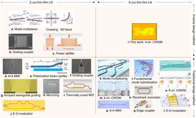
Fig. 1. A four-quadrant diagram of photonics devices based on TFLN. (a ) A spatial-mode multiplexer, a waveguide crossing, and a compact waveguide bend using a 3D gradient-based inverse-design method25. (b ) A grating coupler using particle swarm optimization method26. (c ) A power splitter using Direct binary search method27. (d ) A 4×4 multimode interference (MMI)28. (e ) A polarization beam splitter29. (f ) An alignment-tolerant grating coupler30. (g ) An arrayed waveguide grating31. (h ) A microring resonator for soliton microcomb generation32. (i ) A tunable Mach-Zehnder interferometer (MZI)33. (j ) An integrated electro-optic modulator34. (k ) A mode-multiplexing device35. (l ) A fundamental mode hybridization36. (m ) A 4 channel CWDM device37. (n ) A compact racetrack resonator38. (o ) A lithium niobate photonic chip for wavelength-division-multiplexing transmitters39. (p ) A 4×4 MMI for C-band optical 90-degree hybrid40. (q ) An ultra-broadband and low-loss edge coupler41. (r ) A dual-polarization TFLN in-phase quadrature modulators42. Figure reproduced with permission from: (a) ref.25, Copyright © 2023 American Chemical Society; (b) ref.26, under a Creative Commons Attribution 4.0 International License; (d) ref.28, Copyright © 2021 Optica Publishing Group; (e) ref.29, under a Creative Commons Attribution 4.0 International License; (f) ref.30, Copyright © 2019 Optica Publishing Group; (h) ref.32, Copyright © 2019 Optica Publishing Group; (k) ref.35, Copyright © 2023 John Wiley and Sons; (l) ref.36, Copyright © 2023 Optica Publishing Group; (m) ref.37, Copyright © 2022 Chinese Laser Press; (o) ref.39, under a Creative Commons Attribution 4.0 International License; (p) ref.40, Copyright © 2023 Optica Publishing Group; (r) ref.42, Copyright © 2022 Optica Publishing Group.
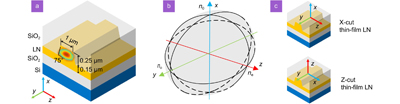
Fig. 2. (a ) Schematic diagram of the three-dimensional structure of X-cut LN waveguide. (b ) Schematic diagram of refractive index ellipsoid. (c ) Schematic diagram of X-cut LN and Z-cut LN.
Fig. 3. (a ) Workflow of the inverse design method for anisotropic materials with the dielectric constant tensor. (b ) Forward simulation of a linear system, b is a point source, F is the objective function at the measuring point, and p is the spatial distribution of the dielectric constant. (c ) Adjoint simulation of a linear system, the point source given by ∂F T/∂x is located at the measuring point.
Fig. 4. (a ) Schematic of the inverse design of a thin-film LN four-channel wavelength division demultiplexer device. (b ) The iterative process of FOM during the inverse design process, including the FOM for the four ports and the total FOM (blue line) of the device. (c ) Spectral response of four output ports verified in FDTD simulation of a structure designed by inverse design using isotropic materials. Inset is the electric field distribution within the design region while the center wavelength of the input optical signal is 1515 nm. (d ) Spectral response of four output ports verified in FDTD simulation of the same structure after setting the material of the structure to the tensor form of X-cut LN. Inset is the electric field distribution within the design region while the center wavelength of the input optical signal is 1515 nm.
Fig. 5. (a ) The iterative process of FOM during the inverse design process using anisotropic materials, including the FOM for the four ports and the total FOM (blue) of the device. (b ) Spectral response of four output ports verified in FDTD simulation of a structure designed by inverse design using anisotropic materials. (c ) The electric field distribution within the design region while the center wavelengths of the input optical signal are 1515 nm, 1535 nm, 1555 nm, and 1575 nm, respectively. (d ) The device structure designed using the scalar-based and the proposed inverse design methods for anisotropic materials, respectively.
Fig. 6. (a ) Spectral response of four output ports verified in FDTD simulation. (b ) The device structure with an initial design region of 25 µm×10 µm. (c ) Electric field distributions within the design region for center wavelengths of the input optical signal at 1515 nm, 1535 nm, 1555 nm, and 1575 nm, respectively.
|
Table 0. Performance comparison of devices between metamaterial-assisted intuition-based method and anisotropic inverse design.
|
Table 0. Performance comparison of two inverse design methods.

Set citation alerts for the article
Please enter your email address
© Copyright 2018-2021 | Chinese Laser Press. All Rights Reserved 沪ICP备15018463号-20