Jiangbo Lyu1、2、†, Tao Zhu1、2、†, Yan Zhou1, Zhenmin Chen1, Yazhi Pi1, Zhengtong Liu1, Xiaochuan Xu2, Ke Xu2、*, Xu Ma3、**, Lei Wang1、***, Zizheng Cao1、****, and Shaohua Yu1
2Department of Electronic and Information Engineering, Harbin Institute of Technology (Shenzhen), Shenzhen 518055, China
3Key Laboratory of Photoelectronic Imaging Technology and System of Ministry of Education of China, School of Optics and Photonics, Beijing Institute of Technology, Beijing 100081, China
Jiangbo Lyu, Tao Zhu, Yan Zhou, Zhenmin Chen, Yazhi Pi, Zhengtong Liu, Xiaochuan Xu, Ke Xu, Xu Ma, Lei Wang, Zizheng Cao, Shaohua Yu. Inverse design for material anisotropy and its application for a compact X-cut TFLN on-chip wavelength demultiplexer[J]. Opto-Electronic Science, 2023, 2(11): 230038
Copy Citation Text
Inverse design focuses on identifying photonic structures to optimize the performance of photonic devices. Conventional scalar-based inverse design approaches are insufficient to design photonic devices of anisotropic materials such as lithium niobate (LN). To the best of our knowledge, this work proposes for the first time the inverse design method for anisotropic materials to optimize the structure of anisotropic-material based photonics devices. Specifically, the orientation dependent properties of anisotropic materials are included in the adjoint method, which provides a more precise prediction of light propagation within such materials. The proposed method is used to design ultra-compact wavelength division demultiplexers in the X-cut thin-film lithium niobate (TFLN) platform. By benchmarking the device performances of our method with those of classical scalar-based inverse design, we demonstrate that this method properly addresses the critical issue of material anisotropy in the X-cut TFLN platform. This proposed method fills the gap of inverse design of anisotropic materials based photonic devices, which finds prominent applications in TFLN platforms and other anisotropic-material based photonic integration platforms.
Integrated photonics plays a key role in optical communications and on-chip optical interconnection, which consists of various photonics devices. Most traditional photonic integration devices are designed by analytical model-based approaches1. During the optimization process, the geometric shapes and material parameters of the photonic devices are usually given by a priori model and optimized by fine-tuning the individual characteristic parameters after several runs of numerical simulations2, therefore the dimensionality of the traditional parametric optimization problem is limited3. In recent years, the development of inverse design for photonics devices has overturned the situation4-8. Different from the traditional forward design approaches, inverse design method seeks the optimal parameter distribution of the photonics device structures in a larger parameter space through intelligent optimization algorithms, which consume fewer computing resources, bringing the performance of the designed photonic devices closer to their limits or the ideal states. Popular intelligent inverse design optimization algorithms include the adjoint method9, genetic algorithm10, particle swarm optimization11, and neural network algorithm12-15. These algorithms have been applied to integrated photonic device design, for example, power division devices16, wavelength division devices17, 18, gratings19, 20, and so on. Inverse design approaches generally focus on optimizing the spatial distribution of dielectric constants of photonic integrated devices for better performance while maintaining a small footprint. Currently, inverse design is widely used in the design of photonic integrated devices based on isotropic materials, including silicon-on-insulator (SOI)21, Si3N422, and Ⅲ-Ⅴ compound semiconductors23.
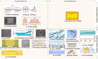
Owing to the CMOS-compatible fabrication process and excellent properties of LN, including strong optical confinement and large nonlinear susceptibilities, the photonic devices based on thin-film lithium niobate (TFLN) have achieved rapid development24. Due to the anisotropy of lithium niobate materials, TFLN devices are usually divided into X-cut and Z-cut types. Within the past five years, different kinds of high-performance photonic integrated devices have been realized on the TFLN platform. Some notable works are summarized in a four-quadrant diagram below25-42.
As shown in Fig. 1, the photonic integrated devices in the left half are based on the Z-cut TFLN designs, while those in the right half are based on the X-cut TFLN. From the lower to the upper half, representative LN integrated photonic devices based on traditional design methods and inverse design methods are displayed, respectively. It is obvious that fewer photonic devices are optimized by inverses design methods. One important reason is that previous inverse design methods cannot deal with the issue of X-cut TFLN anisotropy in the x/y plane. Currently, various X-cut TFLN devices are developed with traditional design methods, as seen in the fourth quadrant. Yet there are no previously published inverse design works for X-cut TFLN devices, as shown in the first quadrant. Although there are a few reports on inverse design for Z-cut TFLN, the issue of material anisotropy is still not addressed. One of the key issues is that the dielectric constant in anisotropic materials is not a scalar identical in all directions as in the isotropic materials, but a tensor43, which is typically represented by a 3×3 diagonal matrix, in which traditional scalar-based inverse design methods are no longer feasible.
Figure 2 briefly depicts the abovementioned X-cut type and Z-cut type of TFLN devices. Figure 2(a) presents a schematic diagram of the three-dimensional structure of X-cut TFLN waveguide, typically passive components are obtained using the wet etching process on the bonded wafers. Figure 2(b) depicts the refractive index ellipsoid of LN. It can be seen that the refractive index values are different along different crystal axes. Therefore, the spatially distributed dielectric constants are depicted as a 3×3 diagonal matrix, which is expressed as
Figure 2.(a) Schematic diagram of the three-dimensional structure of X-cut LN waveguide. (b) Schematic diagram of refractive index ellipsoid. (c) Schematic diagram of X-cut LN and Z-cut LN.
where and respectively represent dielectric constants along the x, y and z directions, and , and . Figure 2(c) shows schematic diagrams of X-cut LN and Z-cut LN. It is noted that when light travels along the y/z plane in an X-cut TFLN device, it encounters two different refractive indices, which is not the case for the Z-cut TFLN devices. As a result, the traditional scalar-based inverse design methods can be applied to the Z-cut TFLN devices, but not to the X-cut ones.
Compared with Z-cut TFLN, X-cut TFLN modulators can make better use of electro-optic coefficient r33 to obtain higher modulation efficiency44-46. To enhance the capacity of the on-chip optical interconnection system, it is crucial for the system to separately modulate light within various wavelength bands. In this scenario, wavelength division demultiplexer devices play a pivotal role in this system. At present, there are two ways to integrate X-cut LN modulators with high modulation efficiency and passive components with other functions. One is to use hybrid integration technology to combine the X-cut TFLN modulator with inverse-designed compact passive devices made of isotropic materials24, 47-49. This practice inevitably increases the fabrication complexity and incurs a higher optical power loss. The other way is to design passive components on the X-cut TFLN platform using traditional design methods, as such they can be fabricated on the same chip together with the modulator. This reduces the processing costs but does not reduce the footprint of the devices. It is desirable to extend the inverse design for X-cut TFLN passive devices.
In this paper, to the best of our knowledge, we report for the first time an inverse design method taking into account optically anisotropic materials and demonstrate its application in designing an ultra-compact TFLN wavelength division demultiplexer device. The implementation of photonics device simulation in the finite-difference time-domain (FDTD) method is achieved by separately handling the three-order diagonal matrix elements of the X-cut TFLN. To validate our approach, we conduct numerical simulations of the wavelength division demultiplexer. The incompatibility of the scalar-based inverse design method on anisotropic X-cut TFLN devices is investigated. We demonstrate the competency of our proposed approach to inverse-designing X-cut TFLN devices, and benchmark their performances with those of isotropic Z-cut TFLN devices using the classical method. Additionally, accounting for dispersion in the waveguide, the device can achieve less crosstalk and lower insertion loss by altering the shape of the simulation area while maintaining the device footprint. This proposed method fills the gap of inverse design of anisotropic materials based photonic devices, which finds prominent applications in TFLN platforms and other anisotropic-material based photonic integration platforms.
Methods
The workflow of the proposed inverse design method is shown in Fig. 3. Figure 3(a) illustrates the workflow of the inverse design algorithm for anisotropic materials, with the dielectric constant tensor serving as a pivotal parameter in this process. After initializing the model, this tensor undergoes normalization. Subsequently, the normalized epsilon is input into the FDTD simulation with forward and adjoint simulation. During each iteration, both a forward simulation and an adjoint simulation are required. In this phase, adjustments to the normalized dielectric constant tensor are made based on the gradients magnitude until either the iteration upper limit is met or optimal results are achieved. During binarization, the Heaviside filter transforms the linear mapping into a step function. During the iteration process, there exists a criterion to determine the completion of binarization, known as ‘discreteness’. Discreteness is determined based on the average value of all normalized dielectric constants in the optimization region. When the discreteness reaches the predefined threshold value, usually 0.999, the binarization process is regarded to be completed, implying that there are only waveguide dielectric constants and background dielectric constants within the optimization area. This leads to the final optimization outcome.
Figure 3.(a) Workflow of the inverse design method for anisotropic materials with the dielectric constant tensor. (b) Forward simulation of a linear system, b is a point source, F is the objective function at the measuring point, and p is the spatial distribution of the dielectric constant. (c) Adjoint simulation of a linear system, the point source given by ∂FT/∂x is located at the measuring point.
Currently, the topology optimization method is widely used in inverse design, which realizes the isotropic inverse design of photonics devices50-52. Generally, this method uses the spatial distribution of the dielectric constant as the object of optimization. By doing so, this method can lead to devices with better performances, because it can provide more optimization parameters by virtue of greater degrees of freedom and larger design space. However, compared with the traditional design methods, topology optimization requires more computational resources and runtime.
To improve the computational efficiency, the adjoint method was introduced to the process of numerical simulation in topology optimization53. Compared with other intelligent optimization algorithms, this method can obtain the gradients of all design parameters in object function with two simulations, thus reducing computational complexity and resource consumption to a large extent, as shown in Fig. 3(b) and 3(c). A brief description of the adjoint method is as follows53.
Assuming the system under consideration consists of linear materials, as shown in Fig. 3(b) and 3(c), the adjoint method requires two simulations to solve for the gradient of the objective function within the optimization region for the design variables. The Maxwell equations can be represented as Eq. (2).
where A is the Maxwell operator, which can be formulated as ; represents the state variables, which might be the electric field E or magnetic field H, represented explicitly as ; b is the source term, whether a current source J or a magnetic dipole M, with its particular form denoted as .
The adjoint equation of the system can be represented as Eq. (3):
where is the adjoint field; F is the objective function, depending on the state variable and the design parameter .
When simulating photonic devices with anisotropic materials, the spatial distribution of the dielectric constant is depicted as a diagonal matrix, which is expressed as Eq. (1). And the bold symbol represents the matrix form of the symbol.
In the adjoint method, the dielectric constant is calculated using the transpose of the diagonal matrix in Eq. (1), and A is represented as Eq. (4):
The forward simulation and adjoint equation of the system are Eq. (5) and Eq. (6), respectively:
Therefore, the gradients of the target function for the design parameters can be expressed as Eq. (7):
where is kth design parameter.
While the dielectric constant does not affect the computational complexity of FDTD simulation, the process of gradients calculation is different. Instead of a single element, it addresses three elements on the diagonal of a third-order matrix, tripling the computational complexity. In the scalar-based inverse design method, the Poynting vector and the wave vector are aligned. However, when anisotropic materials are involved, the Poynting vector and k direction are no longer parallel to each other in general54, 55. Our proposed method effectively resolves the issue by introducing a third-order diagonal permittivity tensor of anisotropic materials in three-dimensional full-vector beam propagation method during the simulation.
Results and discussion
In this section, we demonstrate four types of wavelength division demultiplexers using the scalar-based inverse design method and the proposed inverse design method for anisotropic materials, respectively. The function of a wavelength division demultiplexer is to decompose the input composite optical signal into its constituent signals of individual wavelengths. These optical signals with different center wavelengths can then be separately processed or routed to different waveguides.
A four-channel wavelength division demultiplexer, working in the wavelength range of 1510 nm–1580 nm, is shown in Fig. 4(a). The left channel serves as the input channel of the broadband signal, and on the right are the four output channels. Ports 1, 2, 3, and 4 correspond to the wavelength ranges of 1510 nm–1520 nm, 1530 nm–1540 nm, 1550 nm–1560 nm, and 1570 nm–1580 nm, respectively. Each channel has a designed spectral width of 10 nm. Between each pair of neighboring channels, there is a 10 nm isolation in the wavelength spectrum and a physical spacing of 4 µm between adjacent waveguides. The refractive index of LN material is relatively small, which implies a weaker ability to refract light as compared to silicon-based materials. As a result, wavelength division devices made of LN material tend to have larger dimensions than their silicon-based counterparts. In the initialization, the design area size is set to 16 µm × 16 µm. A slab waveguide is placed in the 16 µm × 16 µm design region with a thickness of 250 nm as the initial structure to allow light transmission from the input end to output ends. The mesh size is set to 50 nm and the minimum feature size is set to 200 nm in both the scalar-based inverse design method and the proposed inverse design method for anisotropic materials. Besides, four frequency monitors are set as figures of merit (FOMs) over the four output ports, which decrease and converge to a fixed value as the iteration number increases. It should be noted these simulation settings are applied throughout this manuscript.
Table Infomation Is Not EnableTable Infomation Is Not Enable
Figure 4.(a) Schematic of the inverse design of a thin-film LN four-channel wavelength division demultiplexer device. (b) The iterative process of FOM during the inverse design process, including the FOM for the four ports and the total FOM (blue line) of the device. (c) Spectral response of four output ports verified in FDTD simulation of a structure designed by inverse design using isotropic materials. Inset is the electric field distribution within the design region while the center wavelength of the input optical signal is 1515 nm. (d) Spectral response of four output ports verified in FDTD simulation of the same structure after setting the material of the structure to the tensor form of X-cut LN. Inset is the electric field distribution within the design region while the center wavelength of the input optical signal is 1515 nm.
In the scalar-based inverse design process, the targeted values of refractive index in the design area are optimized between the waveguide refractive index and the cladding refractive index and eventually binarized. We first set the upper and lower limiting refractive index values to 2.21 and 1.44, respectively, because the refractive index of LN material in TE mode is 2.2151. We then set the target transmittance of the TE mode optical signal as 1 for each port. Here the FOM is the power coupling of guided modes56, as shown in the equation below:
where is the forward transmission of the target light; and are the lower and upper limits of the wavelength points; is the actual mode expansion power transmission; and L is the value of the generalized p-norm.
During the optimization, the overall FOM can be calculated as follows:
where represents the transmittance of each port.
We first obtain an optimized demultiplexer device using traditional inverse design methods, as shown in Fig. 4. During optimization process, the FOMs of ports 2 and 3 drop quickly while FOMs of ports 1 and 4 stays the same. After some iterations, the FOMs of 1 and 4 start to drops. This phenomenon relates to the property of adjoint method. Specific explanations and intermediate processes can be found in the Supplementary information. After 400 steps of optimizations and 200 steps of binarizations, the FOM tends to be stable, and the final values of the four ports are 0.7749, 0.7954, 0.8028, and 0.7672, respectively. Subsequently, we extract the calculated structure and export the GDSII file (refer to Supplementary information) to perform another FDTD simulation for verification. In the verification simulation, we set the refractive index of the inverse design structure to 2.21. As seen in Fig. 4(c), results show that the spectral responses of the four output ports meet the design expectation. Optical signals of different wavelengths are guided to four ports, and the crosstalk between the ports is smaller than −11 dB. The output optical signals of the four ports are spectrally spaced at about 20 nm, and the four ports demonstrate −3 dB bandwidths of 25.6 nm, 19 nm, 18.4 nm, and 35.4 nm, respectively. This is because the total energy of all bands is limited, which imposes constraints on the spectral energy values of Ports 2 and 3 when dividing wavelengths. As a result, the −3 dB bandwidths obtained by Ports 2 and 3 are close to the designed value. In this wavelength division demultiplexer, there are no corresponding restrictions on the wavelength range outside the separation of Port 1 and Port 4. This leads to a much larger bandwidth than the designed parameter.
However, in practice, the refractive index of X-cut LN is not a single value. We replace the refractive index with a tensor form and conduct another verification simulation with the FDTD solver. As shown in Fig. 4(d), unsurprisingly, the results turned out to be quite different and did not meet the design expectations. The overall transmission spectrum is blue-shifted such that output optical signal wavelengths from the ports of interest are not as expected. As can be seen from the electric field distribution diagram in Fig. 4(d), when the wavelength range of the input optical signal is 1510–1520 nm, a considerable part of the light energy propagates to the second port, which is not desired. The crosstalk between the three ports on the right are −7.66 dB, −8.65 dB, −11.07 dB and −8.84 dB, respectively. Therefore, we can see that the scalar-based inverse design is not suitable for anisotropic material systems.
Therefore, we turn to using the proposed inverse design method for anisotropic materials, which calculates the gradients of dielectric constants in a tensor form during the iteration process. In each step of the calculation, the refractive index value at every position within the design region is determined through parameter passing. These parameters are stored in matrix form. By doing so, the anisotropic material is taken into account in the optimization process, while the complexity of the FDTD simulation is not increased.
As we can see from Fig. 5(a), after 400 iterations and 200 binarizations, the FOM tends to level off and no longer changes. We extract the calculated structure to the GDSII file (refer to Supplementary information), set the material to X-cut LN, and perform a verification FDTD simulation, and the result is shown in Fig. 5(b). Since refractive indices of LN materials in the z-axis direction are relatively small, the transmission of each port is about 10% less than that of structures inverse-designed with isotropic materials in the same design region, and the crosstalk values between the ports are −11.96 dB, −11.96 dB, −11.69 dB, and −9.32 dB, respectively. Figure 5(c) visually shows that input optical signals in different wavelength ranges are propagated to their respective output ports, indicating that the device meets the design requirement. Figure 5(d) presents structural diagrams from two inverse design methods: the left depicts a device using the scalar-based inverse design method, while the right illustrates the one using the proposed inverse design method for anisotropic materials. Notably, the structures derived from these two inverse design methods are prominently different from each other. When compared with the X-cut wavelength division demultiplexer shown in Fig. 3(d), there is a marked improvement in the performance of the four ports. This reveals the significant impact of anisotropic materials in the inverse design of photonic devices.
Figure 5.(a) The iterative process of FOM during the inverse design process using anisotropic materials, including the FOM for the four ports and the total FOM (blue) of the device. (b) Spectral response of four output ports verified in FDTD simulation of a structure designed by inverse design using anisotropic materials. (c) The electric field distribution within the design region while the center wavelengths of the input optical signal are 1515 nm, 1535 nm, 1555 nm, and 1575 nm, respectively. (d) The device structure designed using the scalar-based and the proposed inverse design methods for anisotropic materials, respectively.
Moreover, we modify the initial design region from a square to a rectangle, and we also used both methods to design a 25 µm×10 µm wavelength division demultiplexer. For the X-cut TFLN device, results using the proposed method are shown in Fig. 6, and results using the scalar-based inverse design method are displayed in Fig. S2(b). In our design, we consider optimizing the performance of the device within the comparable device footprint. Under this circumstance, the average optical power output of each port has increased by nearly 1 dB, and the crosstalk of four ports are decreased to −17.4 dB, −16.1 dB, −17.5 dB, and −16.5 dB, respectively. Besides, the −3 dB bandwidths of four channels are 32.2 nm, 17.6 nm, 18.1 nm, and 29.3 nm, respectively. These results show that traditional scalar-based inverse design method is not suitable for anisotropic materials e.g., X-cut TFLN. Furthermore, the performances of the X-cut TFLN devices designed by our proposed inverse design method are comparable to those of the Z-cut devices designed by traditional method, which are detailed in Fig. S2(a). The elongated length of the device along the propagation direction amplifies the effect of dispersion in the waveguide, which is more advantageous for the device to realize wavelength division multiplexing and demultiplexing. Such a rectangular structure is more similar to the traditional MMI design structure. Simulation results indicate that the shape of the initial design region can influence the optimization results.
Figure 6.(a) Spectral response of four output ports verified in FDTD simulation. (b) The device structure with an initial design region of 25 µm×10 µm. (c) Electric field distributions within the design region for center wavelengths of the input optical signal at 1515 nm, 1535 nm, 1555 nm, and 1575 nm, respectively.
A comparison of device performances for the two inverse design methods is summarized in Table 1.
As shown in Table 1, wavelength division demultiplexers using the inverse design method for anisotropic materials have a better uniformity for −3 dB bandwidth, center wavelength deviance (Δλ) and insertion loss. Notably, the elongated design device possesses significantly smaller crosstalk values in all ports. On the contrary, the X-cut TFLN device obtained by the scalar-based inverse design method possesses inferior performances on these indicators.
In addition, we compare the performance of the wavelength division demultiplexers obtained by the proposed anisotropic method with those designed by the traditional intuition-based method, as shown in Table 2. As a comparison, the device designed by our proposed method has a prominently 3000 times smaller footprint. The smaller physical intervals between adjacent ports contribute to the larger crosstalk in our designed device.
Conclusions
In this work, we propose a novel inverse design method for photonics devices made of anisotropic materials. Using this method, we design two 1×4 wavelength division demultiplexers. By comparing with the scalar-based inverse design approach, we prove the effectiveness of the proposed inverse design method for anisotropic materials. It should be noted that we do not take the impact of fabrication errors into account, and this method inevitably demands a computational complexity three times greater than the traditional scalar-based approach in the process of data processing. Besides being applied to LN-based material, this novel approach can also be extended to other optically anisotropic materials with enhanced simulation accuracies. It not only provides a more precise prediction of light propagation within these materials in FDTD simulations, but also ensures optimal performance of designed devices to a large extent. This method fills the gap of inverse design in anisotropic materials and lays a solid foundation for the development of anisotropic optoelectronic and photonic devices. Moreover, photonics devices developed using this method might play a significant part in photonic integrated circuits in the future.
Acknowledgements
This work was supported from the Major Key Project of PCL and the National Talent Program.
The authors declare no competing financial interests.
[23] JM Ramirez, H Elfaiki, T Verolet, C Besancon, A Gallet et al. III-V-on-silicon integration: from hybrid devices to heterogeneous photonic integrated circuits. IEEE J Sel Top Quantum Electron, 26, 6100213(2020).
[29] L Zhang, L Zhang, X Fu, L Yang. Compact, broadband and low-loss polarization beam splitter on lithium-niobate-on-insulator using a silicon nanowire assisted waveguide. IEEE Photonics J, 12, 6601906(2020).
[37] GX Chen, ZL Ruan, Z Wang, PC Huang, CJ Guo et al. Four-channel CWDM device on a thin-film lithium niobate platform using an angled multimode interferometer structure. Photonics Res, 10, 8-13(2022).
[41] XY Liu, SQ Gao, C Zhang, Y Pan, R Ma et al. Ultra-broadband and low-loss edge coupler for highly efficient second harmonic generation in thin-film lithium niobate. Adv Photonics Nexus, 1, 016001(2022).
Jiangbo Lyu, Tao Zhu, Yan Zhou, Zhenmin Chen, Yazhi Pi, Zhengtong Liu, Xiaochuan Xu, Ke Xu, Xu Ma, Lei Wang, Zizheng Cao, Shaohua Yu. Inverse design for material anisotropy and its application for a compact X-cut TFLN on-chip wavelength demultiplexer[J]. Opto-Electronic Science, 2023, 2(11): 230038