Journals >Opto-Electronic Science
Contents


2023
Volume: 2 Issue 11
3 Article(s)
Export citation format
Research Articles
Improved spatiotemporal resolution of anti-scattering super-resolution label-free microscopy via synthetic wave 3D metalens imaging
Yuting Xiao, Lianwei Chen, Mingbo Pu, Mingfeng Xu, Qi Zhang, Yinghui Guo, Tianqu Chen, and Xiangang Luo
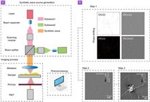
Super-resolution (SR) microscopy has dramatically enhanced our understanding of biological processes. However, scattering media in thick specimens severely limits the spatial resolution, often rendering the images unclear or indistinguishable. Additionally, live-cell imaging faces challenges in achieving high temporal Super-resolution (SR) microscopy has dramatically enhanced our understanding of biological processes. However, scattering media in thick specimens severely limits the spatial resolution, often rendering the images unclear or indistinguishable. Additionally, live-cell imaging faces challenges in achieving high temporal resolution for fast-moving subcellular structures. Here, we present the principles of a synthetic wave microscopy (SWM) to extract three-dimensional information from thick unlabeled specimens, where photobleaching and phototoxicity are avoided. SWM exploits multiple-wave interferometry to reveal the specimen’s phase information in the area of interest, which is not affected by the scattering media in the optical path. SWM achieves ~0.42 λ/NA resolution at an imaging speed of up to 106 pixels/s. SWM proves better temporal resolution and sensitivity than the most conventional microscopes currently available while maintaining exceptional SR and anti-scattering capabilities. Penetrating through the scattering media is challenging for conventional imaging techniques. Remarkably, SWM retains its efficacy even in conditions of low signal-to-noise ratios. It facilitates the visualization of dynamic subcellular structures in live cells, encompassing tubular endoplasmic reticulum (ER), lipid droplets, mitochondria, and lysosomes..
Opto-Electronic Science
- Publication Date: Dec. 30, 2023
- Vol. 2, Issue 11, 230037 (2023)


Inverse design for material anisotropy and its application for a compact X-cut TFLN on-chip wavelength demultiplexer
Jiangbo Lyu, Tao Zhu, Yan Zhou, Zhenmin Chen, Yazhi Pi, Zhengtong Liu, Xiaochuan Xu, Ke Xu, Xu Ma, Lei Wang, Zizheng Cao, and Shaohua Yu
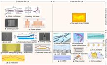
Inverse design focuses on identifying photonic structures to optimize the performance of photonic devices. Conventional scalar-based inverse design approaches are insufficient to design photonic devices of anisotropic materials such as lithium niobate (LN). To the best of our knowledge, this work proposes for the firstInverse design focuses on identifying photonic structures to optimize the performance of photonic devices. Conventional scalar-based inverse design approaches are insufficient to design photonic devices of anisotropic materials such as lithium niobate (LN). To the best of our knowledge, this work proposes for the first time the inverse design method for anisotropic materials to optimize the structure of anisotropic-material based photonics devices. Specifically, the orientation dependent properties of anisotropic materials are included in the adjoint method, which provides a more precise prediction of light propagation within such materials. The proposed method is used to design ultra-compact wavelength division demultiplexers in the X-cut thin-film lithium niobate (TFLN) platform. By benchmarking the device performances of our method with those of classical scalar-based inverse design, we demonstrate that this method properly addresses the critical issue of material anisotropy in the X-cut TFLN platform. This proposed method fills the gap of inverse design of anisotropic materials based photonic devices, which finds prominent applications in TFLN platforms and other anisotropic-material based photonic integration platforms..
Opto-Electronic Science
- Publication Date: Dec. 30, 2023
- Vol. 2, Issue 11, 230038 (2023)

Special issue on digital and intelligent optics
Guangwei Hu, and Junsuk Rho
Opto-Electronic Science
- Publication Date: Dec. 30, 2023
- Vol. 2, Issue 11, 230050 (2023)

© Copyright 2018-2021 | Chinese Laser Press. All Rights Reserved 沪ICP备15018463号-20