• Acta Optica Sinica
  • Vol. 40, Issue 12, 1222001 (2020)
Ci Song1、2、3、*, Ye Tian1、2、3, Feng Shi1、2、3, Kun Zhang1、2、3, and Yongxiang Shen1、2、3
Author Affiliations
  • 1College of Intelligent Science and Technology, National University of Defense Technology, Changsha, Hunan 410073, China
  • 2Hunan Provincial Key Laboratory of Ultra-Precision Machining Technology, Changsha, Hunan 410073 China
  • 3Laboratory of Science and Technology on Integrated Logistics Support, Changsha, Hunan 410073, China
  • show less
    DOI: 10.3788/AOS202040.1222001 Cite this Article Set citation alerts
    Ci Song, Ye Tian, Feng Shi, Kun Zhang, Yongxiang Shen. Process Optimization for Cylindrical Single-Crystal Silicon Mirror with a Tilted Incident Ion Beam Figuring[J]. Acta Optica Sinica, 2020, 40(12): 1222001 Copy Citation Text show less
    Schematic diagram of ion beam figuring
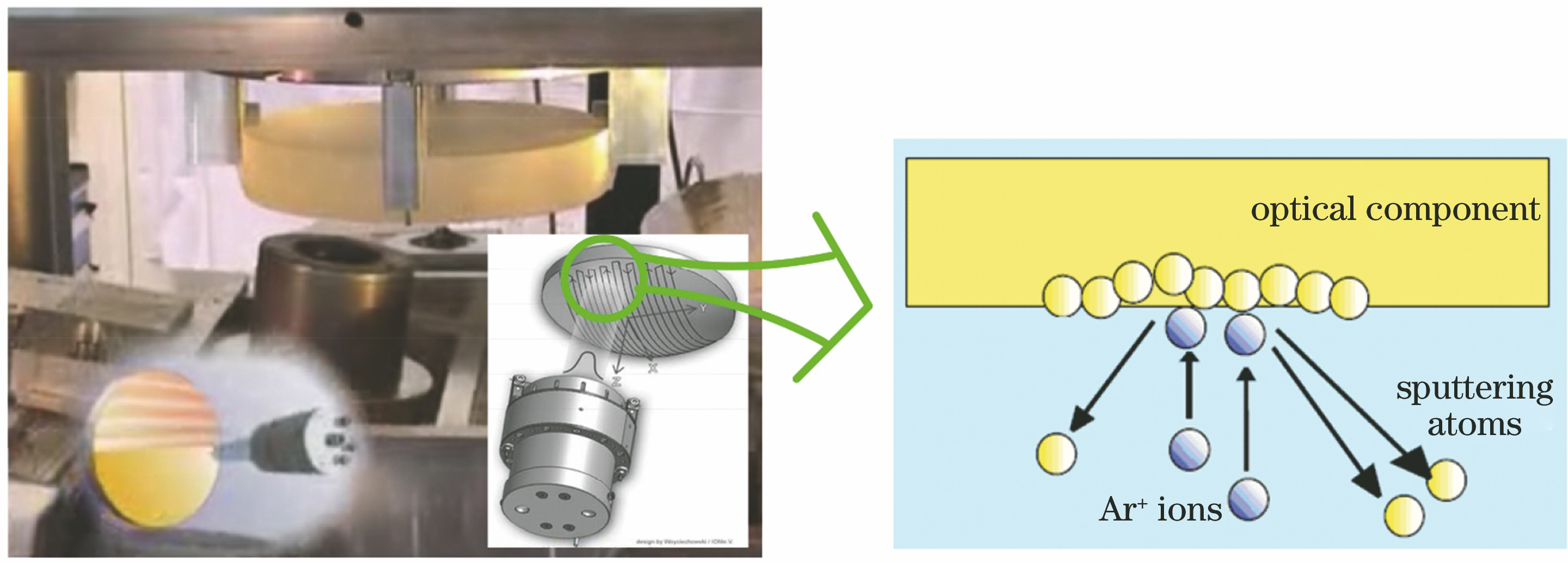
    Fig. 1. Schematic diagram of ion beam figuring
    Schematic diagram of coordinate transformation in tilted incident ion beam figuring process
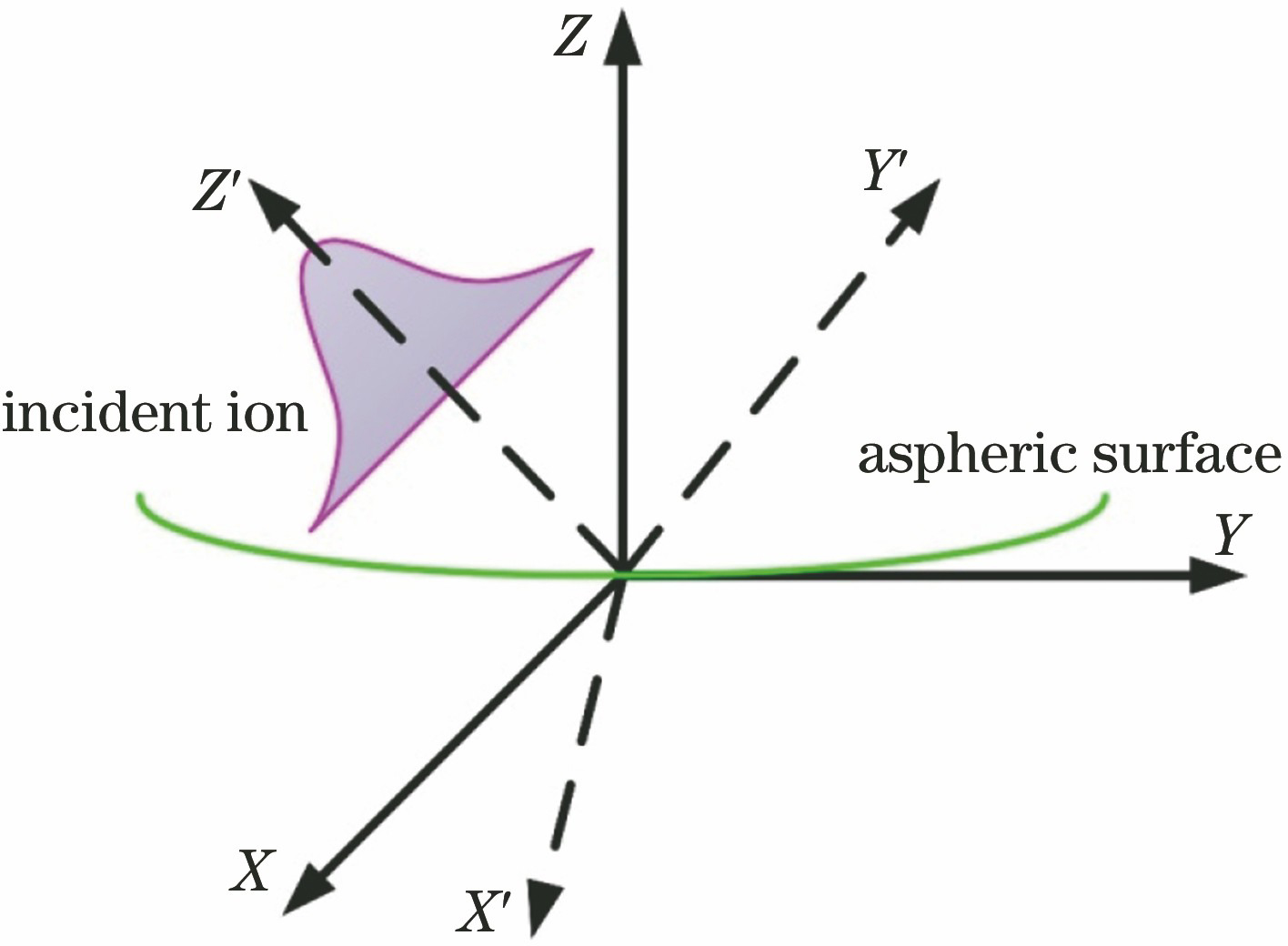
    Fig. 2. Schematic diagram of coordinate transformation in tilted incident ion beam figuring process
    Peak ion beam density varying with the incident angle
    Fig. 3. Peak ion beam density varying with the incident angle
    Normalized beam density distribution versus incident angle (0°, 15°, 30°, 45°, 60°)
    Fig. 4. Normalized beam density distribution versus incident angle (0°, 15°, 30°, 45°, 60°)
    Impact curves of the ion beam incident angle. (a) Peak and volumetric removal rates versus the incident angle; (b) figuring accuracy and dwell time versus the incident angle
    Fig. 5. Impact curves of the ion beam incident angle. (a) Peak and volumetric removal rates versus the incident angle; (b) figuring accuracy and dwell time versus the incident angle
    Impact of local curvature on the ion sputtering
    Fig. 6. Impact of local curvature on the ion sputtering
    Impact of surface gradient on the ion sputtering. (a) Impact of surface gradient on incident angle; (b) secondary sputtering
    Fig. 7. Impact of surface gradient on the ion sputtering. (a) Impact of surface gradient on incident angle; (b) secondary sputtering
    Impact of the incident angle on the ion sputtering
    Fig. 8. Impact of the incident angle on the ion sputtering
    Surface roughness results. (a) Interferometer test results; (b) atomic force microscope test results
    Fig. 9. Surface roughness results. (a) Interferometer test results; (b) atomic force microscope test results
    Tilted incident experiments of ion beam. (a) Experimental photo; (b) surface error map
    Fig. 10. Tilted incident experiments of ion beam. (a) Experimental photo; (b) surface error map
    Surface roughness variation curve. (a) Variation curve with the interferometer test results; (b) variation curve with the atomic force microscope test results
    Fig. 11. Surface roughness variation curve. (a) Variation curve with the interferometer test results; (b) variation curve with the atomic force microscope test results
    Surface roughness variation curves with different incident angles
    Fig. 12. Surface roughness variation curves with different incident angles
    Process flowchart based on the tilted incident ion beam figuring
    Fig. 13. Process flowchart based on the tilted incident ion beam figuring
    Initial surface accuracy and surface roughness of the single crystal silicon cylindrical mirror. (a) Surface error map; (b) surface roughness results with the interferometer test; (c) surface roughness results with the atomic force microscope test
    Fig. 14. Initial surface accuracy and surface roughness of the single crystal silicon cylindrical mirror. (a) Surface error map; (b) surface roughness results with the interferometer test; (c) surface roughness results with the atomic force microscope test
    Surface accuracy and surface roughness with tilted incident ion beam figuring. (a) Surface error map; (b) surface roughness results with the interferometer test; (c) surface roughness results with the atomic force microscope test
    Fig. 15. Surface accuracy and surface roughness with tilted incident ion beam figuring. (a) Surface error map; (b) surface roughness results with the interferometer test; (c) surface roughness results with the atomic force microscope test
    Surface accuracy and surface roughness with vertical incident ion beam figuring. (a) Surface error map; (b) surface roughness results with the interferometer test; (c) surface roughness results with the atomic force microscope test
    Fig. 16. Surface accuracy and surface roughness with vertical incident ion beam figuring. (a) Surface error map; (b) surface roughness results with the interferometer test; (c) surface roughness results with the atomic force microscope test
    Beam voltage /VAnode current /AEmission current /mAAcceleration gate voltage /VGas flow under the standard conditions /(mL·min-1)Mesh size /mmIncident angle /(°)
    8000.8301004300/15/30/45/60
    Table 1. Process parameters in ion beam figuring process
    Ci Song, Ye Tian, Feng Shi, Kun Zhang, Yongxiang Shen. Process Optimization for Cylindrical Single-Crystal Silicon Mirror with a Tilted Incident Ion Beam Figuring[J]. Acta Optica Sinica, 2020, 40(12): 1222001
    Download Citation