Abstract
We investigate the superposition properties of the dipole and quadrupole plasmon modes in the near field both experimentally, by using photoemission electron microscopy (PEEM), and theoretically. In particular, the asymmetric near-field distributions on gold (Au) nanodisks and nanoblocks under oblique incidence with different polarizations are investigated in detail. The results of PEEM measurements show that the evolutions of the asymmetric near-field distributions are different between the excitation with -polarized and -polarized light. The experimental results can be reproduced very well by numerical simulations and interpreted as the superposition of the dipole and quadrupole modes with the help of analytic calculations. Moreover, we hypothesize that the electrons collected by PEEM are mainly from the plasmonic hot spots located at the plane in the interface between the Au particles and the substrate in the PEEM experiments.1. INTRODUCTION
Along with the development of nanotechnology, nanophotonics and plasmonics have drawn much attention over the last few decades. In particular, localized surface plasmon resonance (LSPR) has been extensively investigated because of the wide range of applications [1–4], including in sensors [5,6], photocurrent conversion [7–11], and artificial photosynthesis [12–14]. Recently, many experiments have been reported to provide direct visualization of LSPR using several approaches, such as scanning near-field optical microscopy [15–17], cathodoluminescence microscopy [18,19], electron energy-loss spectroscopy [19–23], and photoemission electron microscopy (PEEM) [24–31]. Among these near-field detection techniques, PEEM utilizes local variations in electron emission to generate image contrast under the excitation of an external light source. PEEM has been demonstrated to be an effective method to investigate the near-field properties of LSPR because of its high spatial resolution (). The near-field enhancement effect of LSPR can promote the process of multiphoton photoemission on the surface of a nanoparticle at the plasmonic hot spots. Therefore, the near-field intensity distribution of LSPR can be directly obtained at a high spatial resolution. Moreover, PEEM also has been used to study the dynamics of dipole and quadrupole LSPR modes integrated with the femtosecond laser pump-probe technique. Using this technique, we previously demonstrated that the quadrupole mode has the longer dephasing time than the dipole mode on the same gold (Au) nanoblocks [25].
The quadrupole mode can be excited for metal nanoparticles such as nanospheres or nanocubes, due to the phase retardation along the light propagation direction [32,33]. For thin planar symmetric metal nanoparticles, the quadrupole mode is normally forbidden with linearly polarized light at normal incidence because of the symmetry selection rules. However, the quadrupole mode on the planar nanoparticles becomes accessible upon the oblique incidence, also due to the phase retardation effect along the nanoparticle plane [34]. Moreover, it has been theoretically studied that the superposition of the dipole mode and the quadrupole mode would break the symmetry of the near-field distribution of LSPR supported by nanoparticles [35,36]. Experimental validation of the spatial evolution of the near-field distribution with high resolution remains challenging. In this paper, we investigate the asymmetric field distribution of LSPR resulting from the superposition of the dipole mode and the quadrupole mode with respect to theoretical work [both analytic calculations and finite difference time-domain (FDTD) numerical simulations] and PEEM experiments. The results show that two types of superposition manners result in the different near-field distributions outside the structures. In addition, the spatial evolution of the asymmetric field distributions with different excitation wavelengths also is investigated. Moreover, the field distributions imaged by PEEM coincide with those on the lower plane located at the interface between the Au structures and the substrate simulated by FDTD. On this basis, we hypothesize that the electrons collected by PEEM are mainly from the plasmonic hot spots at the lower plane in our PEEM experiments. The exact channel electrons ejected through can be inferred, which would provide insight into the mechanism of the multiphoton photoemission process and provide the exact location of the plasmonic hot spots that are important to understanding some applications, such as plasmon-based nonlinear optics and photochemical reactions.
2. SUPERPOSITION OF DIPOLE AND QUADRUPOLE PLASMON RESONANCE
For normal incidence, the conduction electrons of a nanostructure can oscillate coherently. This electronic oscillation mode is called dipole plasmon resonance, where the quasi-static approximation is valid. According to the Laplace equation and the boundary condition, the field distribution of the dipole mode outside the small spherical metal particle can be solved [37]: where is the coefficient of the Legendre function and represents the dipole polarizability, is the radius of the sphere, is the dielectric function of the small spherical metal particle, and is the dielectric function of the surrounding medium. In addition, denotes the electric field outside the particle, denotes the amplitude of the incident light, and , , are the usual unit vectors. To excite the quadrupole mode, symmetry breaking [38] or phase retardation [34,39] has been utilized. In the case of the dipole mode, high order coefficients () of the Legendre function are 0 due to the application of the boundary condition. However, for the quadrupole mode, the term becomes indispensable, and the field outside the sphere is given by [35] where is the wave vector, and is the quadrupole polarizability. From this formula, we find that the electric field distribution outside the particle is a superposition of the dipole (the third term) and quadrupole (the forth term) modes. Because the quadrupole mode has two main angular distributions (odd and even symmetries), two different superposition manners are presented in Fig. 1 qualitatively.
Sign up for Photonics Research TOC. Get the latest issue of Photonics Research delivered right to you!Sign up now
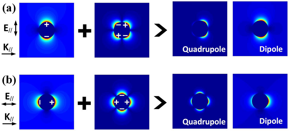
Figure 1.Superposition manners of the dipole and quadrupole modes. (a) The dipole mode couples with the odd symmetric quadrupole mode. (b) The dipole mode couples with the even symmetric quadrupole mode. The “dipole” in the pictures indicates that the dipole mode is dominant. The “quadrupole” in the pictures indicates that the quadrupole mode is dominant. For simple calculations, all distributions are calculated at the plane of and denote the component of the polarization and wave vector parallel to the graph, respectively.
Note that, with the excitation of the quadrupole mode, the superposition of the dipole and quadrupole modes corresponds to an asymmetrical field distribution. Moreover, with different superposition manners, the asymmetrical field distributions have different profiles. Furthermore, the proportions of these two modes in the superposition alter the field distributions for different excitation wavelengths. If the excitation wavelength is near the resonance wavelength of the dipole mode, then the dipole mode is more dominant, and the asymmetric field distribution approaches the dipole mode. Similarly, if the excitation wavelength is near the resonance wavelength of the quadrupole mode, then the quadrupole mode is more dominant and the asymmetric field distribution approaches the quadrupole mode.
3. FAR-FIELD SPECTRA AND NEAR-FIELD MEASUREMENTS
To directly verify the results of the above calculations, the first sample used in the experiments is an Au nanodisk array fabricated on ITO-coated glass by electron-beam lithography [40]. Scanning electron microscopy (SEM) images of the sample are shown in the insets of Fig. 2. The dimensions of the array are , and the thickness of the Au structures is 30 nm. The period is designed to be twice the size of the structures to avoid the grating effect. To observe the respective near-field distribution of the dipole and quadrupole modes, nanodisk samples of two sizes (diameters 280 and 220 nm) are chosen to ensure that the resonance wavelength of the dipole or quadrupole mode is within the tuning range of the pulsed laser source (pulse duration of , and the central wavelength is tunable between 720 and 920 nm), which is used as the excitation light source for the PEEM measurements. The larger structures (280 nm nanodisks) are used to observe the field distributions of the quadrupole mode, and the smaller structures (220 nm nanodisks) are used to observe the dipole mode. The far-field spectra are measured by a Fourier transform infrared (FT-IR) spectrometer [Figs. 2(a) and 2(b)]. A Cassegrainian microscope with the incidence angle spanning between 16° and 32° is used as the objective lens; thus, the incident light is not completely perpendicular to the structure, and the oblique incidence light can excite the quadrupole mode. The main peak shown in the far-field spectrum is the peak of the dipole mode, and the shoulder-like peak represents the quadrupole mode. The near-field intensity spectra are measured using PEEM at grazing incidence angle (74° from normal) through tuning of the wavelength of the laser source step by step [Figs. 2(a) and 2(b)] for both -polarized and -polarized light. The experimental details have been previously reported [25,31,41]. The -polarized light and -polarized light denote the electric field of the light is perpendicular and parallel to the plane of incidence ( plane defined in Figs. 2–5, axis is out of the graphs), respectively. The near-field intensity spectra illustrate that the -polarized laser can excite the dipole and quadrupole modes both efficiently. In addition, the quadrupole mode becomes more dominant with larger nanodisks because of the larger phase retardation. Whereas, for the -polarization, the dipole peak is not pronounced and the quadrupole mode is dominant in the near-field intensity spectrum.

Figure 2.Far-field and near-field intensity spectra of the nanodisk samples with diameters of (a) 280 and (b) 220 nm. Black lines are the far-field spectra measured by FT-IR; the two red lines are the near-field intensity spectra measured by PEEM at oblique incidence with -polarization and -polarization. The curves with -polarization are normalized to that with -polarization. Insets are SEM images; the scale bar is 200 nm.
Figure 3.PEEM images with different light sources. (a) Topography of 280 nm nanodisks imaged with UV light. (b) Field distributions of 280 nm nanodisks exited at the dipole LSPR wavelength (920 nm) with horizontal polarized () laser. (c) Field distributions of 280 nm nanodisks excited at the quadrupole LSPR wavelength (780 nm) with different polarizations. Left: -polarization (). Right: -polarization (). (d) Field distributions of 220 nm nanodisks excited at the dipole LSPR wavelength (820 nm) with different polarizations. Left: -polarization (). Right: -polarization (). Dash circles outline the geometry of the Au nanodisks. All the intensity contrasts in PEEM images have been adjusted to clearly show the distributions.
Figure 4.Field distributions simulated by FDTD and measured by PEEM. (a–c, g–i) Field distributions with -polarization. (d–f, j–l) Field distributions with -polarization. In (a–f), the diameter of the nanodisk is 280 nm; in (g–l), the diameter of the nanodisk is 220 nm. (a, d, g, j) Field distributions on the upper plane of the structures simulated by FDTD. (b, e, h, k) Field distributions on the lower plane of the structures simulated by FDTD. (c, f, i, l) Field distributions measured by PEEM. “Quadrupole” indicates that the distributions are excited with the excitation wavelength near the quadrupole resonance wavelength. “Dipole” indicates that the distributions are excited with the excitation wavelength near the dipole resonance wavelength. All the intensity contrasts in PEEM and simulated images have been adjusted to clearly show the distributions.
Figure 5.Spectra of the nanoblock samples with side lengths of (a) 230 and (b) 200 nm. Black lines are the far-field spectra measured by FT-IR; the two red lines are the near-field intensity spectra measured by PEEM at oblique incidence with -polarization and -polarization. The two curves are normalized to the curve with -polarization. (c) and (d) Field distributions under different wavelengths. First row: Field distributions on the upper plane of the structures simulated by FDTD. Second row: Field distributions on the lower plane of the structures simulated by FDTD. Third row: Field distributions measured by PEEM. “Quadrupole” indicates that the distributions are excited with the laser near the quadrupole resonance wavelength. “Dipole” indicates that the distributions are excited with the laser near the dipole resonance wavelength. Insets are SEM images; the scale bar is 200 nm. All the intensity contrasts in PEEM and simulated images have been adjusted to show the distributions clearly.
For near-field mapping, PEEM with two types of light sources is used to observe the structure topography and the LSPR field distribution. One light source is a UV light source that can be used to image the structure topography, as shown in Fig. 3(a), via the linear photoemission process. Here, the image contrast mechanism is based on the differences of the work function and the carrier density between Au and the ITO substrate [42]. The other light source is a pulsed laser source that can be used to obtain the near-field mapping of LSPR via the multiphoton photoemission process assisted by the near-field enhancement effect. At normal incidence and horizontal polarization (along the axis), the field distribution around the dipole LSPR wavelength at 920 nm [shown in Fig. 3(b)] has two symmetric hot spots around the nanodisk. It is noted that only the dipole mode is excited at normal incidence. When using the oblique incident laser (all oblique laser illumination is from left to right), the near field of the LSPR is redistributed with the excitation of the quadrupole mode. According to the near-field intensity spectra above, we image the field distribution on the nanodisk with different polarizations at the quadrupole LSPR wavelength [Fig. 3(c)] and the dipole LSPR wavelength [Fig. 3(d)], respectively. As seen in Figs. 3(c) and 3(d), the distribution with the -polarized laser corresponds to the analytic calculation results shown in Fig. 1(a) (superposition of the dipole mode and the odd symmetric quadrupole mode). The distribution with the -polarized laser corresponds to the calculation results shown in Fig. 1(b) (superposition of the dipole mode and the even symmetric quadrupole mode). Thus, the results of the calculations and the PEEM measurements are in good agreement. Moreover, in our experiments, upon the irradiation of the femtosecond laser pulses, approximately four-photon photoemission is involved, which is validated by the power-dependent measurements. In this case, the photoemission intensity is proportional to the electric field intensity to the power of 4 [24,25]. As a result, the slight difference in local near-field intensity can cause a large difference in photoemission intensity. This is also the reason accounting for the large variations in the signal strength of different nanodisks in each PEEM image of Figs. 3(b)–3(d).
4. SPATIAL EVOLUTION OF NEAR-FIELD DISTRIBUTION
Moreover, when we change the excitation wavelength, the field distribution on the nanodisk is also reconstructed. To learn more details regarding the variation of the field distribution, we use an FDTD solutions software package (Lumerical, Inc.) to simulate the electric field distribution in the near field. The optical properties of Au are obtained using data from Johnson and Christy [43]. The ITO-coated glass substrate is assumed to behave as a dielectric material with an average refractive index of . The plane wave is irradiated onto the structures at the incidence angle of 74° (the same as PEEM experiments). The Bloch boundary conditions are imposed at and directions, and the perfectly matched layer (PML) boundary conditions are imposed at the direction. The simulation region in plane is chosen the same as the one unit of the array. The mesh size is chosen as 2 nm after convergence test. Two power monitors located at the upper and lower surface of the Au nanostructures are applied to record the electric field.
Figures 4(a), 4(d), 4(g), and 4(j) show the field distributions on the plane located at the upper surface of the structures simulated by FDTD at different wavelengths. For ease of comparison with the PEEM results, the geometrical parameters of the nanodisks designed in FDTD are approximately those of the real nanodisks used in PEEM measurements. When the excitation wavelength is near the quadrupole resonance wavelength, the - or -polarized laser would excite the quadrupole mode dominantly, and the electric field contour has four asymmetric lobes. On the other hand, when the excitation wavelength is near the dipole resonance wavelength, the - or -polarized laser would excite the dipole mode dominantly and the electric field contour has two asymmetric lobes. Comparing the results of FDTD [Figs. 4(a), 4(d), 4(g), and 4(j)] and PEEM [Figs. 4(c), 4(f), 4(i), and 4(l)], we note that the field distributions coincide with each other well at almost all the wavelengths. However, the PEEM images show different variation trend compared with the simulated results when the wavelength of the -polarized laser is tuned toward the red side of the dipole mode. For PEEM images, the electric field located on the left side of the nanodisk becomes gradually stronger, as presented in Fig. 4(l). It is opposite to what the simulated results reveal in Fig. 4(j). To determine the possible reason for this discrepancy, the field distributions on the lower plane located at the interface between the Au nanodisks and the substrate also are simulated, as shown in Figs. 4(b), 4(e), 4(h), and 4(k). It is surprising that the simulated results on the lower plane are in accord with the PEEM results well. At this stage, two questions arise: Why do the results of PEEM coincide with the field distributions on the lower plane? Why are the field distributions on the upper and lower plane are different?
To answer the two questions, we repeat the experiments and simulations using nanoblock samples. The stronger near-field enhancement of the nanoblock is beneficial for PEEM imaging and for observing the spatial evolution of the near-field distribution. In the same way, two structures with different sizes (side lengths: 230 and 200 nm) are used as the samples, and the SEM images are presented in the insets of Fig. 5. The far-field and near-field spectra shown in Figs. 5(a) and 5(b) illustrate that, for nanoblocks, the quadrupole mode is dominant with the -polarized laser, and the dipole mode is dominant with the -polarized laser. Here, we focus on the spatial evolution of the field distribution of the quadrupole mode with 230 nm nanoblocks excited by the -polarized laser and the dipole mode with 200 nm nanoblocks excited by -polarized laser. In terms of near-field mapping, the simulated and PEEM results are also compared with each other. As seen in Figs. 5(c) and 5(d), because of the oblique incidence, the field distributions of the nanoblocks also become asymmetric, and these asymmetric distributions exhibit different spatial variations with the change of the excitation wavelength. The PEEM results show that, for -polarization, the left hot spots disappear gradually with the excitation wavelength moving towards the red side of the quadrupole mode. For -polarization, contrary to the case of -polarization, there are no hot spots on the left of the structures in the blue side of the dipole mode. In the FDTD simulations, we find that the field distributions on the lower plane coincide with the PEEM results. In addition, the phenomenon that the field distributions on the upper and lower plane are different is observed for both nanodisk and nanoblock structures with the -polarized laser.
Some possible explanations for the questions mentioned above are provided as follows. Figure 6(a) presents two main channels, through which electrons are ejected. One channel corresponds to electrons being ejected from the plasmonic hot spots (especially at the corners/edges) of the Au structures on the upper plane. The other channel corresponds to electrons being ejected from the plasmonic hot spots on the lower plane of the Au structures. For the second channel, it is probable for these electrons to be ejected from either Au or the nearby ITO substrate [42]. From the cross section of the electric field distribution of a nanoblock [Fig. 6(b)], the electric field enhancement in the plasmonic hot spots on the lower plane is a little stronger than that on the upper plane. Considering the nonlinearity of the photoemission (for four-photon photoemission process, the photoemission intensity is proportional to the electric field intensity to the power of 4), the photoemission intensity from the plasmonic hot spots on the lower plane would be much stronger. Based on the aforementioned discussions, we hypothesize that the photoelectrons are mainly from the plasmonic hot spots located at the lower plane in our PEEM experiments. Therefore, the field distributions imaged by PEEM correspond more closely to those on the lower plane of the structures simulated by FDTD. For the second question, we note that the field distributions on the upper and lower planes are different only when the structures are illuminated with the -polarized laser. Thus, we believe that the vertical component of the -polarized laser induces the electrons on the left and right side walls of the structure to oscillate with the phase retardation. This phase retardation causes the difference between the upper and lower planes.
Figure 6.Diagram of electron emission and electric field distribution. (a) Possible channels in which electrons are ejected. (b) Simulated cross section of the electric field distribution of the 230 nm nanoblock excited by -polarized laser with the excitation wavelength at 840 nm.
5. CONCLUSION
In summary, we investigated the near-field distribution of LSPR on Au nanodisks and nanoblocks at oblique incidence both experimentally, by using PEEM, and theoretically. Asymmetric field distributions are found in PEEM measurements and FDTD simulations; in particular, the different superposition manners induce different asymmetric field distributions. The analytical calculations reveal that the asymmetric field distributions correspond to the superposition of the dipole mode and quadrupole mode, which is formed because of phase retardation under oblique incidence. Moreover, the spatial evolution of the field distributions under different excitation wavelengths was studied by PEEM measurements and FDTD simulations. It was found that the variation trend of the field distributions imaged by PEEM coincides with the simulated results on the lower plane of the structures, especially for excitation by -polarized light. Possible explanations for this observation were provided based on the contribution of the vertical electric field component and the different near-field enhancement factors between the upper and lower planes of the structures. Our work will help to achieve a deeper understanding of the near-field distribution on the surface of metal nanoparticles; this near-field distribution is important for plasmon-based nonlinear optics and photochemical reaction processes.
Acknowledgment
Acknowledgment. The authors acknowledge the support by the Nanotechnology Platform (Hokkaido University), and Dynamic Alliance for Open Innovation Bridging Human, Environment and Materials (Five-Star Alliance) of MEXT.
References
[1] S. Y. Lee, K. Kim, S. J. Kim, H. Park, K. Y. Kim, B. Lee. Plasmonic meta-slit: shaping and controlling near-field focus. Optica, 2, 6-13(2015).
[2] H. Linnenbank, S. Linden. Second harmonic generation spectroscopy on second harmonic resonant plasmonic metamaterials. Optica, 2, 698-701(2015).
[3] H. W. Jia, F. Yang, Y. Zhong, H. T. Liu. Understanding localized surface plasmon resonance with propagative surface plasmon polaritons in optical nanogap antennas. Photon. Res., 4, 293-305(2016).
[4] R. Tellez-Limon, M. Fevrier, A. Apuzzo, R. Salas-Montiel, S. Blaize. Theoretical analysis of Bloch mode propagation in an integrated chain of gold nanowires. Photon. Res., 2, 24-30(2014).
[5] K. M. Mayer, J. H. Hafner. Localized surface plasmon resonance sensors. Chem. Rev., 111, 3828-3857(2011).
[6] G. J. Nusz, A. C. Curry, S. M. Marinakos, A. Wax, A. Chilkoti. Rational selection of gold nanorod geometry for label-free plasmonic biosensors. ACS Nano, 3, 795-806(2009).
[7] A. P. Kulkarni, K. M. Noone, K. Munechika, S. R. Guyer, D. S. Ginger. Plasmon-enhanced charge carrier generation in organic photovoltaic films using silver nanoprisms. Nano Lett., 10, 1501-1505(2010).
[8] K. Nakamura, T. Oshikiri, K. Ueno, Y. M. Wang, Y. Kamata, Y. Kotake, H. Misawa. Properties of plasmon-induced photoelectric conversion on a TiO2/NiO p-n junction with Au nanoparticles. J. Phys. Chem. Lett., 7, 1004-1009(2016).
[9] X. Shi, K. Ueno, T. Oshikiri, H. Misawa. Improvement of plasmon-enhanced photocurrent generation by interference of TiO2 thin film. J. Phys. Chem. C, 117, 24733-24739(2013).
[10] Y. Tian, T. Tatsuma. Mechanisms and applications of plasmon-induced charge separation at TiO2 films loaded with gold nanoparticles. J. Am. Chem. Soc., 127, 7632-7637(2005).
[11] Z. H. Zhang, L. B. Zhang, M. N. Hedhili, H. N. Zhang, P. Wang. Plasmonic gold nanocrystals coupled with photonic crystal seamlessly on TiO2 nanotube photoelectrodes for efficient visible light photoelectrochemical water splitting. Nano Lett., 13, 14-20(2013).
[12] T. Oshikiri, K. Ueno, H. Misawa. Plasmon-induced ammonia synthesis through nitrogen photofixation with visible light irradiation. Angew. Chem. Int. Ed., 53, 9802-9805(2014).
[13] T. Oshikiri, K. Ueno, H. Misawa. Selective dinitrogen conversion to ammonia using water and visible light through plasmon-induced charge separation. Angew. Chem. Int. Ed., 55, 3942-3946(2016).
[14] Y. Q. Zhong, K. Ueno, Y. Mori, X. Shi, T. Oshikiri, K. Murakoshi, H. Inoue, H. Misawa. Plasmon-assisted water splitting using two sides of the same SrTiO3 single-crystal substrate: conversion of visible light to chemical energy. Angew. Chem. Int. Ed., 53, 10350-10354(2014).
[15] R. Esteban, R. Vogelgesang, J. Dorfmuller, A. Dmitriev, C. Rockstuhl, C. Etrich, K. Kern. Direct near-field optical imaging of higher order plasmonic resonances. Nano Lett., 8, 3155-3159(2008).
[16] Y. Nishiyama, K. Imura, H. Okamoto. Observation of plasmon wave packet motions via femtosecond time-resolved near-field imaging techniques. Nano Lett., 15, 7657-7665(2015).
[17] D. Denkova, N. Verellen, A. V. Silhanek, V. K. Valev, P. Van Dorpe, V. V. Moshchalkov. Mapping magnetic near-field distributions of plasmonic nanoantennas. ACS Nano, 7, 3168-3176(2013).
[18] M. Frimmer, T. Coenen, A. F. Koenderink. Signature of a Fano resonance in a plasmonic metamolecule’s local density of optical states. Phys. Rev. Lett., 108, 077404(2012).
[19] T. Coenen, D. T. Schoen, S. A. Mann, S. R. K. Rodriguez, B. J. M. Brenny, A. Polman, M. L. Brongersma. Nanoscale spatial coherent control over the modal excitation of a coupled plasmonic resonator system. Nano Lett., 15, 7666-7670(2015).
[20] D. Rossouw, M. Couillard, J. Vickery, E. Kumacheva, G. A. Botton. Multipolar plasmonic resonances in silver nanowire antennas imaged with a subnanometer electron probe. Nano Lett., 11, 1499-1504(2011).
[21] V. Myroshnychenko, J. Nelayah, G. Adamo, N. Geuquet, J. Rodriguez-Fernandez, I. Pastoriza-Santos, K. F. MacDonald, L. Henrard, L. M. Liz-Marzan, N. I. Zheludev, M. Kociak, F. J. G. de Abajo. Plasmon spectroscopy and imaging of individual gold nanodecahedra: a combined optical microscopy, cathodoluminescence, and electron energy-loss spectroscopy study. Nano Lett., 12, 4172-4180(2012).
[22] J. Martin, M. Kociak, Z. Mahfoud, J. Proust, D. Gerard, J. Plain. High-resolution imaging and spectroscopy of multipolar plasmonic resonances in aluminum nanoantennas. Nano Lett., 14, 5517-5523(2014).
[23] S. J. Barrow, D. Rossouw, A. M. Funston, G. A. Botton, P. Mulvaney. Mapping bright and dark modes in gold nanoparticle chains using electron energy loss spectroscopy. Nano Lett., 14, 3799-3808(2014).
[24] Q. Sun, K. Ueno, H. Yu, A. Kubo, Y. Matsuo, H. Misawa. Direct imaging of the near field and dynamics of surface plasmon resonance on gold nanostructures using photoemission electron microscopy. Light Sci. Appl., 2, e118(2013).
[25] Q. Sun, H. Yu, K. Ueno, A. Kubo, Y. Matsuo, H. Misawa. Dissecting the few-femtosecond dephasing time of dipole and quadrupole modes in gold nanoparticles using polarized photoemission electron microscopy. ACS Nano, 10, 3835-3842(2016).
[26] F. Schertz, M. Schmelzeisen, R. Mohammadi, M. Kreiter, H. J. Elmers, G. Schonhense. Near field of strongly coupled plasmons: uncovering dark modes. Nano Lett., 12, 1885-1890(2012).
[27] P. Melchior, D. Bayer, C. Schneider, A. Fischer, M. Rohmer, W. Pfeiffer, M. Aeschlimann. Optical near-field interference in the excitation of a bowtie nanoantenna. Phys. Rev. B, 83, 235407(2011).
[28] P. Melchior, D. Kilbane, E. J. Vesseur, A. Polman, M. Aeschlimann. Photoelectron imaging of modal interference in plasmonic whispering gallery cavities. Opt. Express, 23, 31619-31626(2015).
[29] M. Cinchetti, A. Gloskovskii, S. A. Nepjiko, G. Schonhense, H. Rochholz, M. Kreiter. Photoemission electron microscopy as a tool for the investigation of optical near fields. Phys. Rev. Lett., 95, 047601(2005).
[30] B. Y. Ji, J. Qin, H. Y. Tao, Z. Q. Hao, J. Q. Lin. Subwavelength imaging and control of ultrafast optical near-field under resonant- and off-resonant excitation of bowtie nanostructures. New J. Phys., 18, 093046(2016).
[31] H. Yu, Q. Sun, K. Ueno, T. Oshikiri, A. Kubo, Y. Matsuo, H. Misawa. Exploring coupled plasmonic nanostructures in the near field by photoemission electron microscopy. ACS Nano, 10, 10373-10381(2016).
[32] A. B. Evlyukhin, C. Reinhardt, U. Zywietz, B. N. Chichkov. Collective resonances in metal nanoparticle arrays with dipole-quadrupole interactions. Phys. Rev. B, 85, 245411(2012).
[33] O. Nicoletti, F. de la Pena, R. K. Leary, D. J. Holland, C. Ducati, P. A. Midgley. Three-dimensional imaging of localized surface plasmon resonances of metal nanoparticles. Nature, 502, 80-84(2013).
[34] F. Hao, E. M. Larsson, T. A. Ali, D. S. Sutherland, P. Nordlander. Shedding light on dark plasmons in gold nanorings. Chem. Phys. Lett., 458, 262-266(2008).
[35] K. L. Kelly, E. Coronado, L. L. Zhao, G. C. Schatz. The optical properties of metal nanoparticles: the influence of size, shape, and dielectric environment. J. Phys. Chem. B, 107, 668-677(2003).
[36] J. Rodriguez-Fernandez, J. Perez-Juste, F. J. G. de Abajo, L. M. Liz-Marzan. Seeded growth of submicron Au colloids with quadrupole plasmon resonance modes. Langmuir, 22, 7007-7010(2006).
[37] J. D. Jackson. Classical Electrodynamics(1999).
[38] H. Wang, Y. P. Wu, B. Lassiter, C. L. Nehl, J. H. Hafner, P. Nordlander, N. J. Halas. Symmetry breaking in individual plasmonic nanoparticles. Proc. Natl. Acad. Sci. USA, 103, 10856-10860(2006).
[39] Y. C. Chang, S. M. Wang, H. C. Chung, C. B. Tseng, S. H. Chang. Observation of absorption-dominated bonding dark plasmon mode from metal-insulator-metal nanodisk arrays fabricated by nanospherical-lens lithography. ACS Nano, 6, 3390-3396(2012).
[40] K. Ueno, S. Juodkazis, V. Mizeikis, K. Sasaki, H. Misawa. Spectrally-resolved atomic-scale length variations of gold nanorods. J. Am. Chem. Soc., 128, 14226-14227(2006).
[41] O. Lecarme, Q. Sun, K. Ueno, H. Misawa. Robust and versatile light absorption at near-infrared wavelengths by plasmonic aluminum nanorods. ACS Photon., 1, 538-546(2014).
[42] R. C. Word, J. P. S. Fitzgerald, R. Konenkamp. Electron emission in the near-field of surface plasmons. Surf. Sci., 607, 148-152(2013).
[43] P. B. Johnson, R. W. Christy. Optical constants of the noble metals. Phys. Rev. B, 6, 4370-4379(1972).

