• Journal of Semiconductors
  • Vol. 42, Issue 12, 122804 (2021)
Shangfeng Liu1、2, Ye Yuan2, Shanshan Sheng1, Tao Wang4, Jin Zhang2, Lijie Huang2, Xiaohu Zhang2, Junjie Kang2, Wei Luo2, Yongde Li2, Houjin Wang2, Weiyun Wang2, Chuan Xiao2, Yaoping Liu2, Qi Wang3, and Xinqiang Wang1、2
Author Affiliations
  • 1State Key Laboratory of Artificial Microstructure and Mesoscopic Physics School of Physics, Nano-Optoelectronics Frontier Center of Ministry of Education, Peking University, Beijing 100871, China
  • 2Songshan Lake Materials Laboratory, Dongguan 523808, China
  • 3Dongguan Institute of Optoelectronics, Peking University, Dongguan 523808, China
  • 4Electron Microscopy Laboratory, School of Physics, Peking University, Beijing 100871, China
  • show less
    DOI: 10.1088/1674-4926/42/12/122804 Cite this Article
    Shangfeng Liu, Ye Yuan, Shanshan Sheng, Tao Wang, Jin Zhang, Lijie Huang, Xiaohu Zhang, Junjie Kang, Wei Luo, Yongde Li, Houjin Wang, Weiyun Wang, Chuan Xiao, Yaoping Liu, Qi Wang, Xinqiang Wang. Four-inch high quality crack-free AlN layer grown on a high-temperature annealed AlN template by MOCVD[J]. Journal of Semiconductors, 2021, 42(12): 122804 Copy Citation Text show less
    (Color online) The XRD rocking curves (XRC) of (002) (circles) and (102) (squares) planes for (a) as-sputtered and (b) HTA AlN samples.
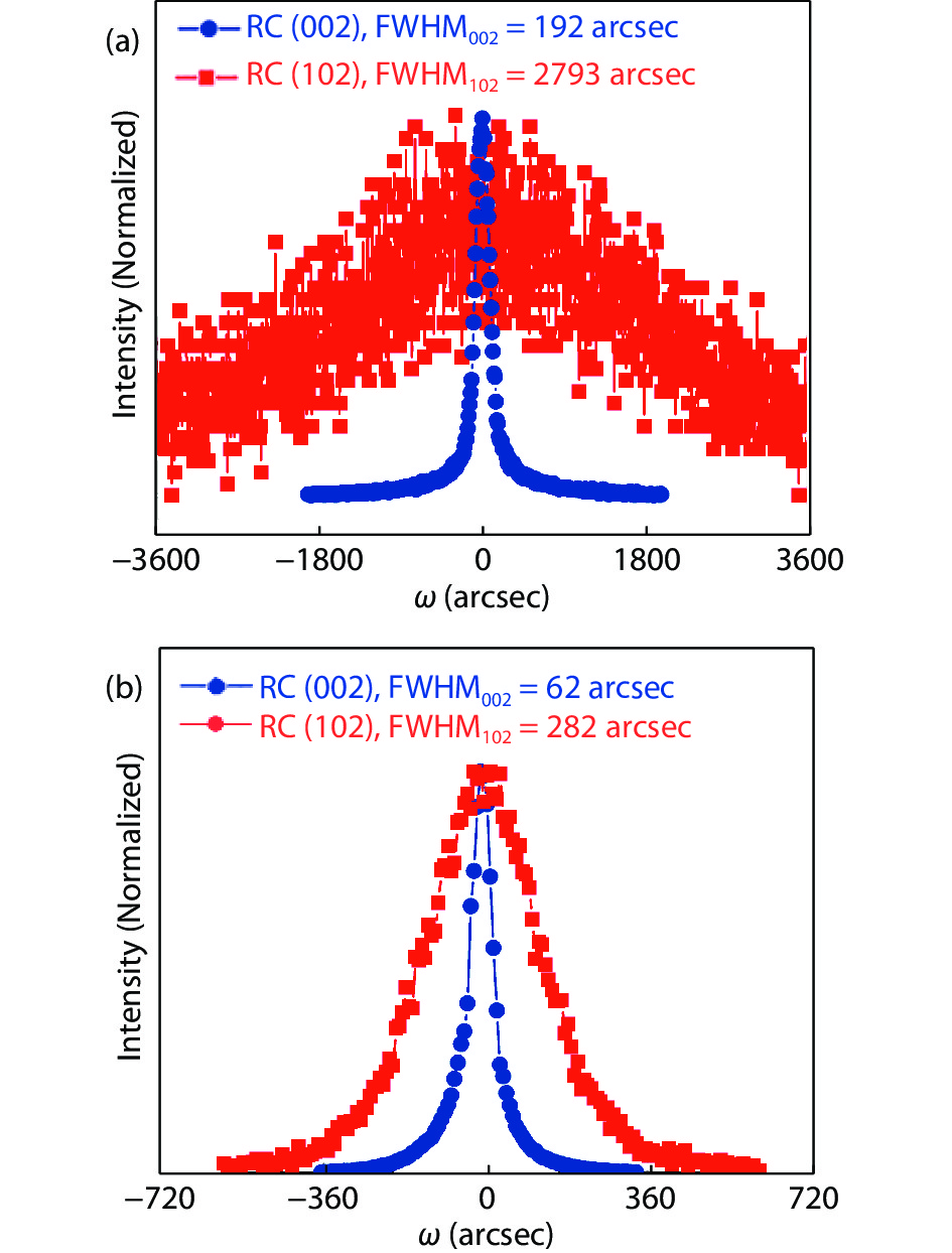
    Fig. 1. (Color online) The XRD rocking curves (XRC) of (002) (circles) and (102) (squares) planes for (a) as-sputtered and (b) HTA AlN samples.
    Cross-sectional weak-beam dark-field (WBDF) TEM images of HTA AlN taken under diffraction conditions of (a) g = () and (b) g = (). For g = ()/(), the screw-type/edge-type dislocation is visible. (c) Cross-sectional high-resolution HAADF-STEM along the [] direction by focusing on the interfacial region.
    Fig. 2. Cross-sectional weak-beam dark-field (WBDF) TEM images of HTA AlN taken under diffraction conditions of (a) g = ( ) and (b) g = ( ). For g = ( )/( ), the screw-type/edge-type dislocation is visible. (c) Cross-sectional high-resolution HAADF-STEM along the [ ] direction by focusing on the interfacial region.
    (Color online) Atomic force microscopy images of (a) as-sputtered AlN, (b) HTA AlN as well as (c) MOCVD regrown AlN. (d) The SEM image of MOCVD regrown AlN on HTA AlN template. The height bar is 20 nm.
    Fig. 3. (Color online) Atomic force microscopy images of (a) as-sputtered AlN, (b) HTA AlN as well as (c) MOCVD regrown AlN. (d) The SEM image of MOCVD regrown AlN on HTA AlN template. The height bar is 20 nm.
    (Color online) (a) Positions of five measured XRC points on 4-inch as-sputtered AlN and MOCVD regrown AlN wafers, and the results are shown in Table 1. (b) Optical microscopy image of the edge region in MOCVD regrown AlN wafer on 4-inch HTA AlN template. The images of surface cracks on (c) HTA AlN and (d) AlN/NPSS templates are measured by Candela.
    Fig. 4. (Color online) (a) Positions of five measured XRC points on 4-inch as-sputtered AlN and MOCVD regrown AlN wafers, and the results are shown in Table 1. (b) Optical microscopy image of the edge region in MOCVD regrown AlN wafer on 4-inch HTA AlN template. The images of surface cracks on (c) HTA AlN and (d) AlN/NPSS templates are measured by Candela.
    PositionHTA AlN FWHM (002)/(102)(arcsec) Regrown AlN FWHM (002)/(102)(arcsec) Regrown AlN strain // c (%)
    187 / 310162 / 3810.0869
    264 / 28895 / 3720.0799
    357 / 28385 / 3200.0795
    461 / 31078 / 3120.0795
    570 / 32189 / 3290.0807
    Table 1. Five points XRC FWHMs and θω calculated strains of 4-inch post-HTA AlN and MOCVD regrown AlN wafers.
    Shangfeng Liu, Ye Yuan, Shanshan Sheng, Tao Wang, Jin Zhang, Lijie Huang, Xiaohu Zhang, Junjie Kang, Wei Luo, Yongde Li, Houjin Wang, Weiyun Wang, Chuan Xiao, Yaoping Liu, Qi Wang, Xinqiang Wang. Four-inch high quality crack-free AlN layer grown on a high-temperature annealed AlN template by MOCVD[J]. Journal of Semiconductors, 2021, 42(12): 122804
    Download Citation