
Shangfeng Liu, Ye Yuan, Shanshan Sheng, Tao Wang, Jin Zhang, Lijie Huang, Xiaohu Zhang, Junjie Kang, Wei Luo, Yongde Li, Houjin Wang, Weiyun Wang, Chuan Xiao, Yaoping Liu, Qi Wang, Xinqiang Wang. Four-inch high quality crack-free AlN layer grown on a high-temperature annealed AlN template by MOCVD[J]. Journal of Semiconductors, 2021, 42(12): 122804
- Journal of Semiconductors
- Vol. 42, Issue 12, 122804 (2021)
Abstract
1. Introduction
The explosive spread of the coronavirus disease (COVID-19) in the 2019 pandemic intensively excites the requirement for high-efficiency environmental sterilization that interrupts the most important link in the chain of disease transmission. Although plenty of conventional methods have been used, e.g. alcohol immersion, high-temperature treatment, as well as high-energy irradiation, AlGaN-based ultraviolet-C (UVC, λ ≤ 280 nm) light-emitting diode (LED) disinfection is emerging as one of the most promising and convincing avenues to confront COVID-19[
From the viewpoint of industry and commercialization, the employment of economical AlN template, a 4-inch scaled wafer in particular would be more attractive if it exhibits the possibility to further reduce the cost of UVC-LED: (i) the cost would be intensively decreased by using crack-free 4-inch AlN template which has never been achieved to date; and (ii) the previously necessary epitaxial thickness of 3–4 µm (to acquire the qualified flat morphology and high crystalline quality for subsequent device epitaxy) would be avoided and largely save the expense of device epitaxy.
In this work, by combining the physical vapor deposition (PVD) and face-to-face HTA technique, for the first time, a 4-inch single-crystalline AlN template whose dislocation density is as low as 9.2 × 108 cm–2 level is achieved. On the basis of the HTA AlN template, the MOCVD regrowth of homo-epitaxial AlN layer at the 4-inch wafer scale is initialized, highlighting the prospective of wafer-sized HTA AlN templates in UVC irradiation source revolution.
2. Experiment
Four-inch AlN wafers were prepared on c-plane sapphires by reaction magneto-sputtering technique using aluminum (purity ~ 99.999%) as the target, and the sputtering ambient was set as the mixture of argon and nitrogen as a ratio of 1 : 4. The AlN thickness was set as 500 nm by calibrating the growth speed and the sputtering power was 3000 W. Afterwards, as-sputtered AlN wafers were annealed by utilizing a tube furnace at 1700 °C for over 5 h, and the annealing ambient was nitrogen with a flow rate of 0.5 SLM. The MOCVD AlN regrowth was performed by a Prismo HiT3 MOCVD system at a temperature of 1200 °C. The regrown thickness is 200 nm. The rocking curves of AlN (002) and (102) planes were measured by X-ray diffraction (XRD, Brucker D8 Discovery) to evaluate the AlN crystallinity. High-angle annular dark-field scanning transmission electron microscopy (HAADF-STEM) was carried out in a Thermo fisher FEI Themis Z Cs probe-corrected STEM system operated at 300 kV, weak-beam dark-field (WBDF) TEM was observed using Tecnai F30 at 300 kV. The scanning electron microscopy (SEM, Hitachi Regulus 8100) and atomic force microscopy (AFM, Veeco DimensionTM 3100) with a typing mode were used to explore the surface morphology of all AlN samples.
3. Results and discussion
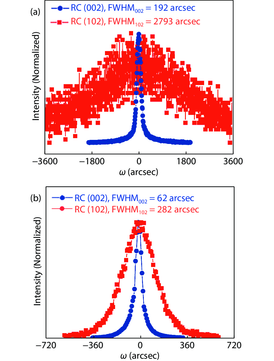
Fig. 1 shows XRD rocking curves (XRC) of (002) and (102) planes of as-sputtered and HTA AlN. Before the HTA treatment, the as-sputtered AlN presents c-oriented characteristic. The full width at half maximum (FWHM) of (002) and (102) XRC are 192 and 2793 arcsec, respectively, which are comparable with the values of previously reported as-Al target-sputtered[
![]()
Figure 1.(Color online) The XRD rocking curves (XRC) of (002) (circles) and (102) (squares) planes for (a) as-sputtered and (b) HTA AlN samples.
where the Ddis represents the density of dislocation, b is the length of Burgers vector, with values of 0.4982 and 0.3112 nm for screw- and edge-type dislocations, respectively;
To capture more information of the HTA AlN, the dark field cross-sectional TEM measurement was adopted, with two beam conditions carried out to analyze dislocations in different types. As shown in Figs. 2(a) and 2(b), the screw-type dislocation is nonvisible while only two edge-type dislocation lines are seen in the scanned area. Such low dislocation density agrees with XRC results. To analyze the dislocation annihilation driven by HTA operation, high-resolution HAADF-STEM was performed, focusing on the interfacial region between HTA AlN and sapphire. From the Fig. 2(c), an atomically sharp interface between sapphire and HTA AlN is visible and demonstrates a nice epitaxial nature in the high temperature treated AlN/sapphire system. However, a color-contrast region around 10 nm away from the interface is detected as a boundary between sapphire-neared N-polar AlN and upper Al-polar AlN. Actually, such a depth has been observed and verified as inversion domain boundary which consists of compound (111) γ-AlON[
![]()
Figure 2.Cross-sectional weak-beam dark-field (WBDF) TEM images of HTA AlN taken under diffraction conditions of (a)
In addition to the prospective from the application point of view, a series of fundamental experience, which possibly deepens the understand of high temperature AlN regrowth, particularly the contribution from oxides cooperation[
The morphologies of as-sputtered, post-annealed, as well as MOCVD-regrown, AlN were studied by AFM, and the results are shown in Fig. 3. The as-sputtered AlN presents the columnar-morphology which is the same as the previously reported AlN film prepared by magneto-sputtering[
![]()
Figure 3.(Color online) Atomic force microscopy images of (a) as-sputtered AlN, (b) HTA AlN as well as (c) MOCVD regrown AlN. (d) The SEM image of MOCVD regrown AlN on HTA AlN template. The height bar is 20 nm.
When compared with a 2-inch wafer, the 4-inch AlN layer grown on sapphire by MOCVD generally exhibits larger bow and terrible cracks which is detrimental to upper epilayers and acts as the main obstacle to large-sized device epitaxy[
![]()
Figure 4.(Color online) (a) Positions of five measured XRC points on 4-inch as-sputtered AlN and MOCVD regrown AlN wafers, and the results are shown in Table 1. (b) Optical microscopy image of the edge region in MOCVD regrown AlN wafer on 4-inch HTA AlN template. The images of surface cracks on (c) HTA AlN and (d) AlN/NPSS templates are measured by Candela.
Table Infomation Is Not Enable4. Conclusion
In summary, the pronounced single-crystalline 4-inch AlN templates with dislocation density as low as 9.2 × 108 cm–2 on the c-plane sapphire are achieved. Thanks to such high-quality AlN template, the MOCVD regrown AlN with the thickness of only 700 nm shows comparative quality as the 3–4 µm AlN layer grown by ELOG. The exhibiting bunching-step morphology and low dislocation density in the regrown 4-inch AlN layer prove its qualification of being an ideal candidate substrate for low-cost UVC-LEDs.
Acknowledgements
This work was supported by the Key-Area Research and Development Program of Guangdong Province (Nos. 2019B121204004 and 2019B010132001), Science Challenge Project (No. TZ2018003), Basic and Application Basic Research Foundation of Guangdong Province (No. 2020A1515110891) and the National Natural Science Foundation of China (Nos. 61734001 and 61521004).
References
[1] I H Hamzavi, A B Lyons, I Kohli et al. Ultraviolet germicidal irradiation: Possible method for respirator disinfection to facilitate reuse during the COVID-19 pandemic. J Am Acad Dermatol, 82, 1511(2020).
[2] A E Torres, A B Lyons, S Narla et al. Ultraviolet-C and other methods of decontamination of filtering facepiece N-95 respirators during the COVID-19 pandemic. Photochem Photobiol Sci, 19, 746(2020).
[3] S F Liu, W Luo, D Li et al. Sec-eliminating the SARS-CoV-2 by AlGaN based high power deep ultraviolet light source. Adv Funct Mater, 31, 2008452(2021).
[4] Y Kashima, N Maeda, E Matsuura et al. High external quantum efficiency (10%) AlGaN-based deep-ultraviolet light-emitting diodes achieved by using highly reflective photonic crystal on p-AlGaN contact layer. Appl Phys Express, 11, 012101(2018).
[5] D Wang, K Uesugi, S Y Xiao et al. Low dislocation density AlN on sapphire prepared by double sputtering and annealing. Appl Phys Express, 13, 095501(2020).
[6] H Miyake, C H Lin, K Tokoro et al. Preparation of high-quality AlN on sapphire by high-temperature face-to-face annealing. J Cryst Growth, 456, 155(2016).
[7] C Y Huang, P Y Wu, K S Chang et al. High-quality and highly-transparent AlN template on annealed sputter-deposited AlN buffer layer for deep ultra-violet light-emitting diodes. AIP Adv, 7, 055110(2017).
[8] R Yoshizawa, H Miyake, K Hiramatsu. Effect of thermal annealing on AlN films grown on sputtered AlN templates by metalorganic vapor phase epitaxy. Jpn J Appl Phys, 57, 01AD05(2018).
[9] J Hakamata, Y Kawase, L Dong et al. Growth of high-quality AlN and AlGaN films on sputtered AlN/sapphire templates via high-temperature annealing. Phys Status Solidi B, 255, 1700506(2018).
[10] K Uesugi, K Shojiki, Y Tezen et al. Suppression of dislocation-induced spiral hillocks in MOVPE-grown AlGaN on face-to-face annealed sputter-deposited AlN template. Appl Phys Lett, 116, 062101(2020).
[11] N Susilo, E Ziffer, S Hagedorn et al. Improved performance of UVC-LEDs by combination of high-temperature annealing and epitaxially laterally overgrown AlN/sapphire. Photon Res, 8, 589(2020).
[12] N Susilo, S Hagedorn, D Jaeger et al. AlGaN-based deep UV LEDs grown on sputtered and high temperature annealed AlN/sapphire. Appl Phys Lett, 112, 041110(2018).
[13] S Hagedorn, S Walde, A Mogilatenko et al. Stabilization of sputtered AlN/sapphire templates during high temperature annealing. J Cryst Growth, 512, 142(2019).
[14] S Y Xiao, R Suzuki, H Miyake et al. Improvement mechanism of sputtered AlN films by high-temperature annealing. J Cryst Growth, 502, 41(2018).
[15] M X Wang, F J Xu, N Xie et al. High-temperature annealing induced evolution of strain in AlN epitaxial films grown on sapphire substrates. Appl Phys Lett, 114, 112105(2019).
[16] W Gu, Z B Liu, Y N Guo et al. Comprehensive study of crystalline AlN/sapphire templates after high-temperature annealing with various sputtering conditions. J Semicond, 41, 122802(2020).
[17] T Metzger, R Höpler, E Born et al. Defect structure of epitaxial GaN films determined by transmission electron microscopy and triple-axis X-ray diffractometry. Philos Mag A, 77, 1013(1998).
[18] B N Pantha, R Dahal, M L Nakarmi et al. Correlation between optoelectronic and structural properties and epilayer thickness of AlN. Appl Phys Lett, 90, 241101(2007).
[19] J E Ayers. The measurement of threading dislocation densities in semiconductor crystals by X-ray diffraction. J Cryst Growth, 135, 71(1994).
[20] V Srikant, J S Speck, D R Clarke. Mosaic structure in epitaxial thin films having large lattice mismatch. J Appl Phys, 82, 4286(1997).
[21] R Chierchia, T Böttcher, H Heinke et al. Microstructure of heteroepitaxial GaN revealed by X-ray diffraction. J Appl Phys, 93, 8918(2003).
[22] H Heinke, V Kirchner, S Einfeldt et al. X-ray diffraction analysis of the defect structure in epitaxial GaN. Appl Phys Lett, 77, 2145(2000).
[23] X Q Wang, S B Che, Y Ishitani et al. Threading dislocations in In-polar InN films and their effects on surface morphology and electrical properties. Appl Phys Lett, 90, 151901(2007).
[24] S Hagedorn, S Walde, A Knauer et al. Status and prospects of AlN templates on sapphire for ultraviolet light-emitting diodes. Phys Status Solidi A, 217, 1901022(2020).
[25] W M Yim, R J Paff. Thermal expansion of AlN, sapphire, and silicon. J Appl Phys, 45, 1456(1974).
[26] H Fukuyama, H Miyake, G Nishio et al. Impact of high-temperature annealing of AlN layer on sapphire and its thermodynamic principle. Jpn J Appl Phys, 55, 05FL02(2016).
[27] T Akiyma, M Uchino, K Nakamura et al. Structural analysis of polarity inversion boundary in sputtered AlN films annealed under high temperatures. Jpn J Appl Phys, 58, SCCB30(2019).
[28] T Kamohara, M Akiyama, N Ueno et al. Influence of sputtering pressure on polarity distribution of aluminum nitride thin films. Appl Phys Lett, 89, 243507(2006).
[29] J Kaur, N Kuwano, K R Jamaludin et al. Electron microscopy analysis of microstructure of postannealed aluminum nitride template. Appl Phys Express, 9, 065502(2016).
[30] A Yoshikawa, T Nagatomi, T Morishita et al. High-quality AlN film grown on a nanosized concave-convex surface sapphire substrate by metalorganic vapor phase epitaxy. Appl Phys Lett, 111, 162102(2017).
[31] Y Hayashi, K Tanigawa, K Uesugi et al. Curvature-controllable and crack-free AlN/sapphire templates fabricated by sputtering and high-temperature annealing. J Cryst Growth, 512, 131(2019).
[32] J W Ben, X J Sun, Y P Jia et al. Defect evolution in AlN templates on PVD-AlN/sapphire substrates by thermal annealing. CrystEngComm, 20, 4623(2018).
[33] A Uedono, K Shojiki, K Uesugi et al. Annealing behaviors of vacancy-type defects in AlN deposited by radio-frequency sputtering and metalorganic vapor phase epitaxy studied using monoenergetic positron beams. J Appl Phys, 128, 085704(2020).
[34] K Uesugi, Y Hayashi, K Shojiki et al. Reduction of threading dislocation density and suppression of cracking in sputter-deposited AlN templates annealed at high temperatures. Appl Phys Express, 12, 065501(2019).
[35] K Uesugi, Y Hayashi, K Shojiki et al. Fabrication of AlN templates on SiC substrates by sputtering-deposition and high-temperature annealing. J Cryst Growth, 510, 13(2019).
[36] K Shojiki, K Uesugi, S Kuboya et al. High-quality AlN template prepared by face-to-face annealing of sputtered AlN on sapphire. Phys Status Solidi B, 258, 2000352(2021).
[37] I Bryan, Z Bryan, S Mita et al. Surface kinetics in AlN growth: A universal model for the control of surface morphology in III-nitrides. J Cryst Growth, 438, 81(2016).
[38] N Okada, N Kato, S Sato et al. Growth of high-quality and crack free AlN layers on sapphire substrate by multi-growth mode modification. J Cryst Growth, 298, 349(2007).
[39] R G Banal, Y Akashi, K Matsuda et al. Crack-free thick AlN films obtained by NH3Nitridation of sapphire substrates. Jpn J Appl Phys, 52, 08JB21(2013).

Set citation alerts for the article
Please enter your email address
© Copyright 2018-2021 | Chinese Laser Press. All Rights Reserved 沪ICP备15018463号-20