
Daniel Benedikovic, Léopold Virot, Guy Aubin, Farah Amar, Bertrand Szelag, Bayram Karakus, Jean-Michel Hartmann, Carlos Alonso-Ramos, Xavier Le Roux, Paul Crozat, Eric Cassan, Delphine Marris-Morini, Charles Baudot, Frédéric Boeuf, Jean-Marc Fédéli, Christophe Kopp, Laurent Vivien. 25 Gbps low-voltage hetero-structured silicon-germanium waveguide pin photodetectors for monolithic on-chip nanophotonic architectures[J]. Photonics Research, 2019, 7(4): 437
- Photonics Research
- Vol. 7, Issue 4, 437 (2019)
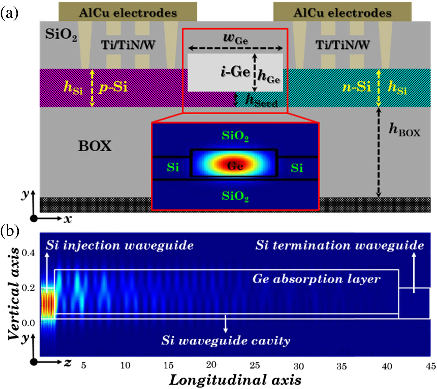
Fig. 1. (a) Transversal schematics (x - y y - z
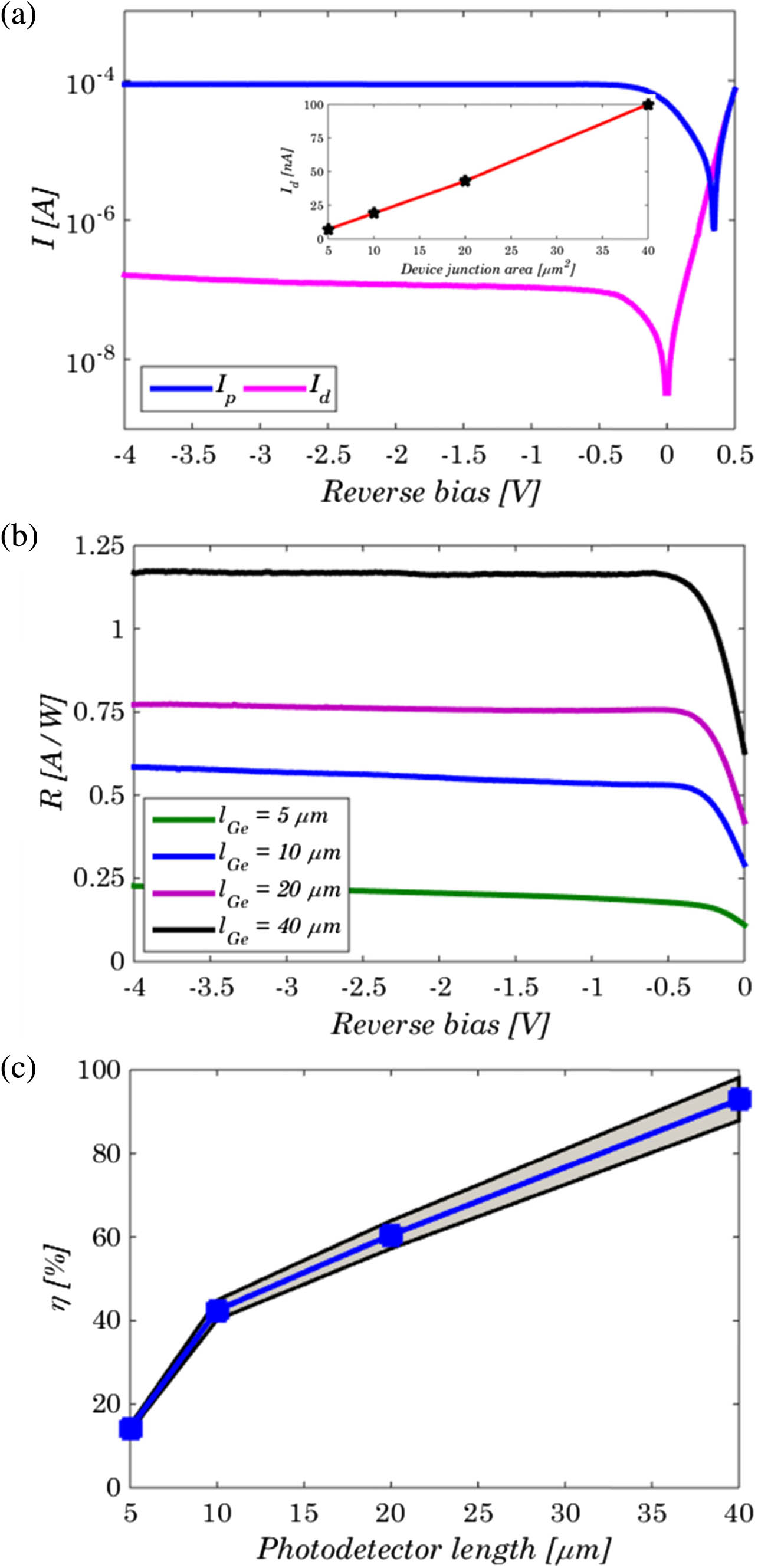
Fig. 2. (a) Static current-voltage (I –V ) characteristics of 1-μm-wide by 40-μm-long hetero-structured pin photodetector in dark- and light-illuminated states. Inset: leakage dark-current evolution as a function of device junction area. Photodetectors were biased at − 1 V − 0.5 V ± 0.24 dB
Fig. 3. (a) Small-signal RF measurements of the S 21 1 - μm - wide × 40 - μm - long − 4 V S 21 − 1 V ± 0.24 dB
Fig. 4. Evolution of eye diagram apertures within a low-reverse-bias range at 10 Gbps, 20 Gbps, 25 Gbps, 28 Gbps, 32 Gbps, and 40 Gbps. Here, x y 1 - μm × 40 - μm Ge width × Ge length
Fig. 5. Bit-error-rate measurements of the Si-Ge-Si pin waveguide photodetector as a function of the input optical power. BER assessments performed (a) at 10 Gbps under low-reverse-bias states and (b) at 10 Gbps, 20 Gbps, and 25 Gbps, all biased at − 3 V 1 - μm × 40 - μm Ge width × Ge length

Set citation alerts for the article
Please enter your email address
© Copyright 2018-2021 | Chinese Laser Press. All Rights Reserved 沪ICP备15018463号-20