
Xiaoxiang Lu, Yong Wang, Xiaomei Han, Zhanguo Li. Study on Light Extraction Efficiency of Enhanced OLED with Nanopatterns[J]. Laser & Optoelectronics Progress, 2018, 55(2): 022301
- Laser & Optoelectronics Progress
- Vol. 55, Issue 2, 022301 (2018)
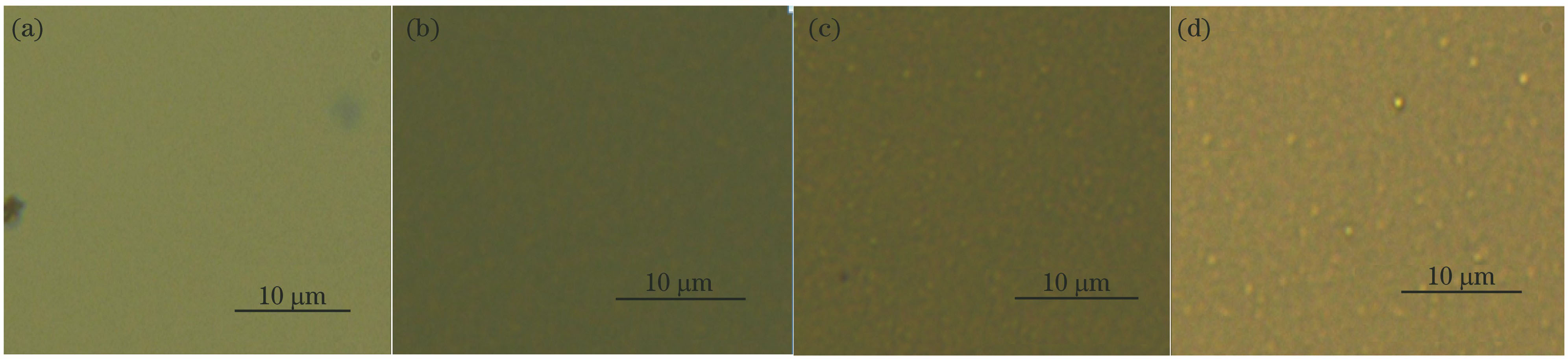
Fig. 1. Optical micrographs with the gold film thickness of (a) 3 nm, (b) 6 nm, (c) 8 nm, (d) 10 nm, while the annealing temperature is 570 ℃ and the annealing time is 210 s
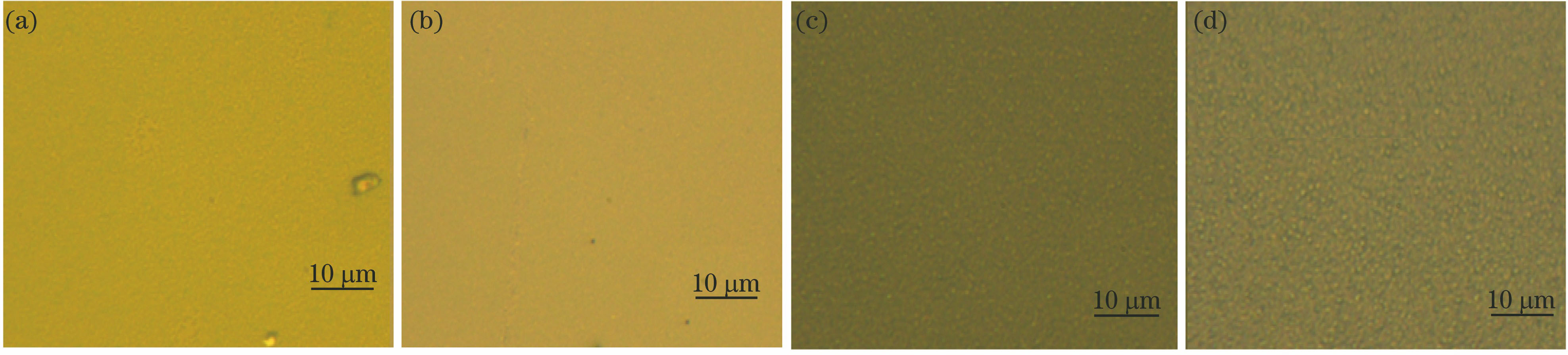
Fig. 2. Optical micrographs with the annealing temperature of (a) 500 ℃, (b) 550 ℃, (c) 570 ℃, (d) 600 ℃ while the gold film thickness is 10 nm
Fig. 3. Optical micrographs with the annealing time of (a) 0 s, (b) 180 s, (c) 210 s, (d) 240 s, while the gold film thickness is 10 nm and the annealing temperature is 570 ℃
Fig. 4. SEM images with the annealing time of (a) 0 s, (b) 180 s, (c) 210 s, (d) 240 s, while the gold film thickness is 10 nm and the annealing temperature is 570 ℃
Fig. 5. (a) SEM image and (b) AFM image of the ITO surfaces etched for 4 min, while the annealing time is 240 s
Fig. 6. Transmittance of the ITO with different etching time
Fig. 7. Current density-voltage curves
Fig. 8. Luminance-voltage curves
Fig. 9. Power efficiency-luminance curves
Fig. 10. Current efficiency-luminance curves
Fig. 11. EL spectra

Set citation alerts for the article
Please enter your email address
© Copyright 2018-2021 | Chinese Laser Press. All Rights Reserved 沪ICP备15018463号-20