• Laser & Optoelectronics Progress
  • Vol. 59, Issue 19, 1900003 (2022)
Qiang Huang1、2, Yi Zhang1, Junqiang Sun1、*, Changliang Yu3, Jianfeng Gao1, Peilin Jiang1, Haotian Shi1, and Chukun Huang1
Author Affiliations
  • 1Wuhan National Laboratory for Optoelectronics, Huazhong University of Science and Technology, Wuhan 430074, Hubei, China
  • 2Hunan Provincial Key Laboratory of Grids Operation and Control on Multi-Power Sources Area, School of Electrical Engineering, Shaoyang University, Shaoyang 422000, Hunan, China
  • 3Wuhan Fisilink Microelectronics Technology Co., Ltd., Wuhan 430040, Hubei, China
  • show less
    DOI: 10.3788/LOP202259.1900003 Cite this Article Set citation alerts
    Qiang Huang, Yi Zhang, Junqiang Sun, Changliang Yu, Jianfeng Gao, Peilin Jiang, Haotian Shi, Chukun Huang. Research Progress on Ge/SiGe Multiple Quantum Well Optical Modulators[J]. Laser & Optoelectronics Progress, 2022, 59(19): 1900003 Copy Citation Text show less
    Band structures of different materials. (a) Si; (b) Ge
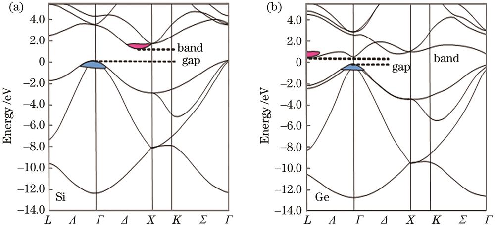
    Fig. 1. Band structures of different materials. (a) Si; (b) Ge
    QCSE in Ge/SiGe quantum well. (a) Without electric field; (b) with electric field applied
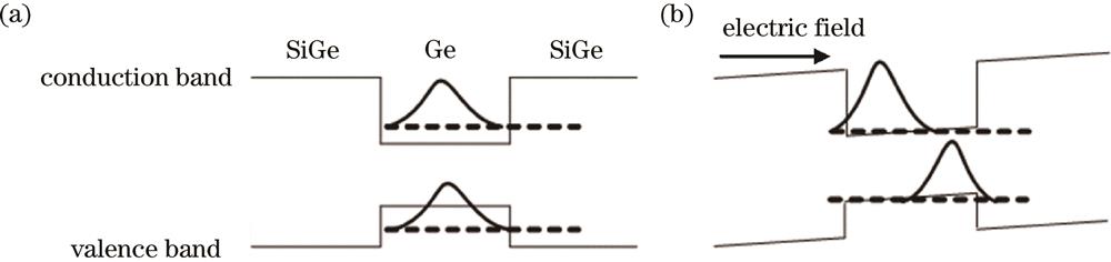
    Fig. 2. QCSE in Ge/SiGe quantum well. (a) Without electric field; (b) with electric field applied
    Epitaxial structure and test results of Ge/SiGe multiple quantum wells. (a) Epitaxial structure; (b) absorption spectra of Ge/SiGe quantum wells[45]
    Fig. 3. Epitaxial structure and test results of Ge/SiGe multiple quantum wells. (a) Epitaxial structure; (b) absorption spectra of Ge/SiGe quantum wells[45]
    Schematic diagram of oblique incidence photoelectric modulator[49]
    Fig. 4. Schematic diagram of oblique incidence photoelectric modulator[49]
    Side oblique incidence Ge/SiGe multiple quantum well modulator. (a) Absorption spectrum at 100 ℃; (b) schematic diagram of the structure[50]
    Fig. 5. Side oblique incidence Ge/SiGe multiple quantum well modulator. (a) Absorption spectrum at 100 ℃; (b) schematic diagram of the structure[50]
    Waveguide type Ge/SiGe multiple quantum well electro-absorption modulator. (a) Epitaxial structure; (b) SEM image; (c) absorption spectra at different voltages; (d) extinction ratio at different operating voltages[28]
    Fig. 6. Waveguide type Ge/SiGe multiple quantum well electro-absorption modulator. (a) Epitaxial structure; (b) SEM image; (c) absorption spectra at different voltages; (d) extinction ratio at different operating voltages[28]
    Test results of Ge/SiGe multiple quantum wells. (a) Absorption spectrum; (b) extinction ratio at different working voltages[31]
    Fig. 7. Test results of Ge/SiGe multiple quantum wells. (a) Absorption spectrum; (b) extinction ratio at different working voltages[31]
    Absorption spectra of Ge/SiGe multiple quantum wells. (a) Absorption spectra of Ge/SiGe multiple quantum wells with different well widths; (b) absorption spectra of Ge/SiGe multiple quantum wells at different voltages[29]
    Fig. 8. Absorption spectra of Ge/SiGe multiple quantum wells. (a) Absorption spectra of Ge/SiGe multiple quantum wells with different well widths; (b) absorption spectra of Ge/SiGe multiple quantum wells at different voltages[29]
    Structure and simulation results of low bias voltage Ge/SiGe multiple quantum well electroabsorption modulator. (a) Structural design; (b) TM polarization absorption coefficient; (c) TE polarization absorption contrast at different voltages[51]
    Fig. 9. Structure and simulation results of low bias voltage Ge/SiGe multiple quantum well electroabsorption modulator. (a) Structural design; (b) TM polarization absorption coefficient; (c) TE polarization absorption contrast at different voltages[51]
    Simulation results of Ge/SiGe multiple quantum well electro-absorption optical modulator. (a) Waveguide structure; (b) overall structure; (c) photocurrent response at different voltages when uniaxial tensile strain is introduced; (d) photocurrent contrast at different voltages[52]
    Fig. 10. Simulation results of Ge/SiGe multiple quantum well electro-absorption optical modulator. (a) Waveguide structure; (b) overall structure; (c) photocurrent response at different voltages when uniaxial tensile strain is introduced; (d) photocurrent contrast at different voltages[52]
    Structure of the modulator. (a) Epitaxial design of multiple quantum wells; (b) overall structure of the device; (c) distribution of biaxial tensile strain[53]
    Fig. 11. Structure of the modulator. (a) Epitaxial design of multiple quantum wells; (b) overall structure of the device; (c) distribution of biaxial tensile strain[53]
    Electroabsorption light modulation extinction ratio of the device under different reverse voltages. (a) 0 V/2 V; (b) 0 V/4 V; (c) high frequency response characteristic curve of the device under TE polarization; (d) high frequency response characteristic curve of the device under TM polarization[53]
    Fig. 12. Electroabsorption light modulation extinction ratio of the device under different reverse voltages. (a) 0 V/2 V; (b) 0 V/4 V; (c) high frequency response characteristic curve of the device under TE polarization; (d) high frequency response characteristic curve of the device under TM polarization[53]
    Test results of Ge/SiGe multiple quantum wells under different bias voltages. (a) Absorption spectrum; (b) secondary electro-optic coefficient[54]
    Fig. 13. Test results of Ge/SiGe multiple quantum wells under different bias voltages. (a) Absorption spectrum; (b) secondary electro-optic coefficient[54]
    Test results of Ge/SiGe asymmetrically coupled multiple quantum wells. (a) FP interference comb spectra at different bias voltages; (b) optical power spectra at different bias voltages; (c) modulation extinction ratios at different operating voltage swings; (d) normalized high-frequency response curve[57]
    Fig. 14. Test results of Ge/SiGe asymmetrically coupled multiple quantum wells. (a) FP interference comb spectra at different bias voltages; (b) optical power spectra at different bias voltages; (c) modulation extinction ratios at different operating voltage swings; (d) normalized high-frequency response curve[57]
    Ref.3 dB modulation bandwidth /GHzInsertion loss /dBExtinction ratio(wavelength)QW structure(thickness)
    4510 periods of Ge(10 nm)/Si0.15Ge0.85(16 nm)
    48Si0.175Ge0.825(5 nm), Ge QW(12.5 nm)
    497.3 dB(1457 nm)40 periods of Ge(15.5 nm)/Si0.16 Ge0.84(33 nm)
    506 dB(1541 nm)10 periods of Ge(15 nm)/Si0.16 Ge0.84(33 nm)
    28239 dB(1435 nm)
    315 dB(1550 nm)Ge QW(14 nm)18 nm(SiGe barrier thickness)
    296 dB(1490 nm)13.6 nm(QW thickness)
    51-7.420.3 dB(1550 nm)
    5211.317.8 dB(1550 nm)
    538.7-37.59.3 dB(1485 nm)
    Table 1. Performance of Ge/SiGe multiple quantum well modulators based on electroabsorption effect
    Ref.3 dB modulation bandwidth /GHzInsertion loss /dBExtinction ratio(wavelength)QW structureElectrorefractive index(wavelength)
    54width(100 μm), length(64 μm)1.3×10⁻³(1475 nm)
    55Ge well(7 nm), Si0.15Ge0.85 internal barrier(1.5 nm)2.3×10⁻³
    569×10-3(1461 nm)
    57327.8 dB(1530 nm)3.2×10⁻³(1530 nm)
    Table 2. Performance comparison of Ge/SiGe multiple quantum well modulators based on electrorefractive index effect
    Qiang Huang, Yi Zhang, Junqiang Sun, Changliang Yu, Jianfeng Gao, Peilin Jiang, Haotian Shi, Chukun Huang. Research Progress on Ge/SiGe Multiple Quantum Well Optical Modulators[J]. Laser & Optoelectronics Progress, 2022, 59(19): 1900003
    Download Citation