1Jiangsu Key Laboratory of Advanced Laser Materials and Devices, School of Physics and Electronic Engineering, Jiangsu Normal University, Xuzhou 221116, China
2Center for Photochemical Sciences, Department of Physics and Astronomy, Bowling Green State University, Bowling Green, Ohio 43403, USA
3College of Materials Science and Engineering, Nanjing Tech University, Nanjing 210009, China
4School of Mechanical Engineering, Jiangsu University, Zhenjiang 212013, China
5School of Materials Science and Engineering, Georgia Institute of Technology, Atlanta, Georgia 30332, USA
Transparent ceramics are emerging as future materials for lasers, scintillation, and illumination. In this paper, an interesting and surprising phenomenon in YAG transparent ceramics is reported. UV light leads to significant changes in the microstructure of open volume defects and nano clusters as well as in the optical properties. Light-induced lattice relaxation is suggested as the mechanism behind this intriguing behavior. The complex F-type color center with broad absorption bands is caused by the aliovalent sintering additives () and Fe ion impurities. Two individual peaks in the thermoluminescence spectra illustrate both shallow and deep level traps. From positron annihilation lifetime data, vacancy clusters and nanovoids are detected and characterized, although these free-volume defects could not be observed by high-resolution transmission electron microscopy. The solarization induced by UV irradiation is associated with a change in the structure and size of defect clusters due to lattice relaxation. Therefore, this work shows how UV irradiation leads not only to a change in the charge state of defects, but also to a permanent change in defect structure and size. It significantly affects the optical properties of YAG ceramics and their performance in lasers and other optical applications. These results are crucial for advancing transparent ceramics technology.
1. INTRODUCTION
Since the first laser oscillation was realized in -doped (Nd:YAG) transparent ceramics by A. Ikesue et al. in 1995 [1,2], various transparent ceramic materials such as garnet (Yb/Nd:YAG) [3,4], sesquioxide () [5,6], and non-oxide (Cr:ZnS, tellurite) [7] have attracted tremendous attention. Transparent ceramics provide homogeneous and large dopant concentrations, and can be easily fabricated in large scales, which is crucial for numerous applications. YAG transparent ceramics have proven to be the best laser host material due to their relatively simple preparation and excellent physical and chemical properties [8–10]. In fact, enormous prospective applications are predicted for this material; however, these potential applications require perfect transparency and minimum light scattering. The most primary scattering losses in transparent YAG ceramics are caused by vacancies, nanopores, and possible secondary phases in grain boundaries. Indeed, even at levels greater than a few ppm (parts per million), these defects form color centers [11,12], leading to a solarization phenomenon during laser operation [13–15], which can decrease the transparency of the gain medium and degrade laser oscillation performance. In the development stages of Nd:YAG single crystal, solarization had been a serious problem [16] with the source of the color center absorption bands attributed to trapped electrons at oxygen vacancy () sites [17]. However, this is no longer as critical of an issue as it once was for YAG single crystals [18,19]. The relationship of color center concentration with impurity ions of variable valence, aliovalent ionic substitutions, and oxygen partial pressure () has also been emphasized in a series of papers [20,21].
Compared to single crystals, there are relatively few studies of defects in transparent ceramics with some carried out on La:[22] and Mg:[23]. For YAG transparent ceramics, Haneda et al.[24] proposed an off stoichiometric cation model for the formation of and showed that these defects resulted in color centers that could be annihilated at grain boundaries and sample surfaces during air annealing. Patel et al.[18] showed that non-stoichiometric YAG was accommodated by antisite defects, while Zych et al.[25] concluded that the color centers and point defects, but not the grain boundaries, were the primary sources of degraded scintillation performance of Ce:YAG ceramics. Yagi et al.[13] attributed the increased absorption in YAG ceramic to doping, which was required to achieve transparency. In the reducing condition of hot isostatic pressing (HIP) sintering, the dark coloration was caused by and could be removed by air annealing [26]. However, this is paradoxical with the fact that the defect mechanism of substitution in YAG lattice would lead to the formation of , not , and thus have little effect on F centers, which are the predominant color centers. One point is very clear: the defect formation has a strong relationship with the sintering additives and sintering conditions in the fabrication of YAG ceramics.
Recently, we developed highly transparent YAG ceramics by vacuum sintering using the divalent sintering additives ( and ) without the commonly used [27,28]; its optical transmittance reached nearly the theoretical value. Considering that color centers deleteriously affect the performance in laser and scintillation applications, it is crucial to study defect behaviors and color center formation in these YAG ceramics. In this work, optical absorption spectroscopy, positron annihilation lifetime spectroscopy (PALS), and thermoluminescence (TL) spectroscopy were combined to study point defects, solarization effect, and trapping kinetics in highly transparent YAG ceramics. The physical nature of defects and microstructure of YAG ceramics are revealed in this work to guide and advance the development of transparent ceramics.
Sign up for Photonics Research TOC. Get the latest issue of Photonics Research delivered right to you!Sign up now
2. MATERIALS AND EXPERIMENTAL DETAILS
A. Preparation of YAG Ceramics
High-purity (99.99% purity, Sumitomo Chemicals, Tokyo, Japan) and (99.99%, Alfa Aesar, MA) powders were used as starting materials, and precisely weighed in stoichiometric proportions to form ceramics. CaO (99.999%, Alfa Aesar, Ward Hill, MA) and MgO (99.999%, Alfa Aesar, Ward Hill, MA) were selected as sintering additives. The molar ratio of Ca and Mg was 1:4, and their total amount was kept at 0.2 mol% according to content. The details about vacuum sintering method can be found elsewhere [27,28]. The powders and sintering additives were mixed with ethyl alcohol and planetary ball milled for 15 h using agate balls ( purity). The milled slurry was dried at 55°C in an oven for 24 h, and then sieved though a 200 mesh screen. After that, the sieved powders were uniaxially pressed at 20 MPa using a stainless-steel mold with a diameter of 16 mm and cold isostatically pressed at 200 MPa to obtain compacted green bodies. The green bodies were then calcined at 900°C for 5 h to remove the organic residues. The final sintering process was carried out at 1840°C for 8 h, followed by annealing in air at 1350°C for 10 h. After that, the samples were mirror polished on both surfaces to 3.0 mm thickness.
B. Characterization
The optical transmittance and absorption of transparent YAG ceramics before and after UV irradiation were measured using a UV-VIS-NIR spectrophotometer (Lambda 950, Perkin-Elmer, Waltham, MA, USA) in the wavelength range of 200–1100 nm. The microstructure of the ceramics was studied by scanning electron microscopy (SEM, JSM-6510, JEOL, Japan) and transmission electron microscopy (TEM, Fecnai-G2-F20, USA). UV irradiation was conducted in the dark using the full power of a pulsed xenon lamp. TL measurements of UV-irradiated ceramics were carried out using an in-house spectrometer that enabled the direct recording of the luminescence as a function of wavelength and temperature [29,30]. After UV irradiation, the lamp was turned off and the emission in the range of 200–800 nm was recorded during a linear-ramp heating from to 400°C with a heating rate of 60°C/min.
Positron lifetime spectra were obtained by sandwiching a source between two identical samples and measured using a fast–fast coincidence spectrometer. The spectrometer is described in more detail elsewhere [31,32]. A minimum of counts was achieved in all the spectra, and each measurement was repeated five to six times. The spectra were fitted with LT software [33] with three Gaussian functions used to describe the resolution function. The numerical positron lifetimes , , and , as well as , , and , were obtained from the exponential fit.
3. RESULTS AND DISCUSSION
A. Optical Measurements and Solarization Effect
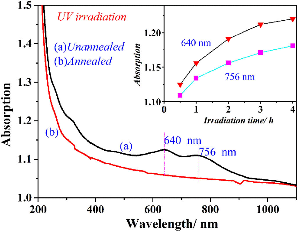
The effect of UV irradiation on the optical absorption of (a) unannealed, and (b) high-temperature (1350°C for 10 h) annealed YAG transparent ceramics is shown in Fig. 1 (data were normalized). The double absorption bands of 640 nm and 756 nm were observed in the spectrum of the unannealed sample [curve (a)]; however, they were completely suppressed in the annealed one [curve (b)]. Compared to the absorption spectra of ceramics before UV irradiation [not shown here due to the complete overlap with curve (b)], the absorption bands formed only in the non-annealed ceramics after UV irradiation. This indicates that the formation of color centers is caused by pre-existing defects in the ceramics that can be mitigated via high-temperature annealing. The inset in Fig. 1 shows the increase in these two absorption bands with the increase in irradiation time. The absorbance of both bands increased and reached saturation when the irradiation time was more than 3 h. The rise of the 756 nm band was relatively slower than that of the 640 nm band after 2 h of irradiation. In fact, after just 30 min of irradiation, the intensities of the two bands reached 90% of the saturation intensity, and any subsequent increases were very small. The defects responsible for the two bands were apparently already present in the samples, and UV irradiation induced a change only in their charge states. Aside from the two obvious bands, there was additional disparity in the overall absorption in the wavelength range of 200–600 nm.
Figure 1.Optical absorption of (a) as-fabricated and (b) high-temperature (1350°C for 10 h) annealed YAG transparent ceramics after UV irradiation (inset: variation with the irradiation time).
The absorption difference between pre- and post-UV irradiation of unannealed ceramics is shown in Fig. 2. Assuming a superposition of Gaussian bands, at least four distinct bands were extracted using a least-squares fitting of the absorption spectrum as represented by the four Gaussian bands in Fig. 2. These bands were peaked at 318 nm, 487 nm, 640 nm, and 756 nm, respectively. Because the wide absorption bands in the visible range were mainly in the green and red regions, the UV-irradiated YAG ceramic was dark blue in color, as shown in the inset in Fig. 2. This indicates the presence of many complex defect types in the unannealed YAG ceramic. Curiously, this blue color is not a common color in YAG optical materials; it is a new color center not previously observed in YAG single crystal or transparent ceramics [13,16,17,34].
Figure 2.Gaussian fitting of optical absorption of colored YAG ceramics using least-squares method.
The solarization effect and its related color centers were first identified by Bass and Paladino [16]; they observed an absorption band from 300 nm to 600 nm in YAG and YGaG single crystals after irradiation with a Xe flashlamp. After, Mori [17] used time-resolved transient absorption spectroscopy to study the absorption bands of transient (833 nm), (495 nm), and (353 nm), and stable peaks at room temperature (253 nm), (312 nm), (403 nm), and (543 nm). They proposed a model based on electron trapping at sites and concluded that , , and formed due to the appearance of color centers based on electron spin resonance (ESR) data. Among the stable , , , and bands, one of them () is related to the center induced by a change in the charge state of iron ions (very common impurity in YAG). represents the charge transfer band, and the other two bands are unidentified donor centers. Zych et al.[25] compared the photoluminescence of YAG:Ce single crystal and ceramics and concluded that there is only one color center in ceramics in the 180–300 nm range. However, Yagi et al.[13] have reported on the increase of absorption at 250–400 nm in YAG ceramics with a additive, which was extended to 250–700 nm after UV irradiation due to the formation of additional . They also observed discoloration in YAG ceramics prepared under reducing conditions, which was bleached by annealing in air. has been identified as a color source, but its doping is critical to achieve high transparency for ceramics. More importantly, the mechanism of doping in YAG lattice should not lead to the formation of : This means doping should have little effect on the formation of F centers. This is also supported by Stevenson’s reports [34,35], which have shown that the absorption of 250–400 nm extended to 250–700 nm in as-sintered ceramics after UV irradiation, but no specific defect was identified because the peak was very weak. This is inconsistent with the strong absorption observed here in Fig. 2. This solarization due to the strong absorption bands at 640 nm and 756 nm is observed only in the as-sintered YAG ceramics using and as sintering additives. The inductively coupled plasma-atomic emission spectrometer (ICP-AES) results confirmed that 83 ppm Fe was found in sample in tetrahedral () and octahedral () coordinated sites. In this case, Fe as an impurity ion with variable valence would have the following oxidation and reduction reactions: This indicates that was increased by reducing the variable valence of impurity ions under low oxygen partial pressure (). It should be mentioned that in the current study, YAG ceramics were sintered in high vacuum, and thus a large number of were formed in the as-sintered ceramics. The absorption band of (318 nm) in Fig. 2 also indicates the presence of [17,36]. Meanwhile, the divalent sintering additives ( and ) would also introduce according to the defect reaction: This further indicates that the aliovalent substitution creates , which is consistent with the increased oxygen diffusivity and the increase in aliovalent substitution in Refs. [20,21]. From the above analysis, it can be concluded that in the current study, a large amount of were present in the vacuum sintered ceramics. During UV irradiation, the oxygen ions are ionized [17,36], and photo-oxidation of leads to the formation of free electrons [36]: All the released electrons are trapped at the pre-existing . This leads to the formation of color center trapped electrons at anion vacancies ( or ) and a corresponding number of hole centers (). Because the optical transition of hole centers within states is forbidden and cannot cause high oscillation strength, the absorption bands of 640 nm and 756 nm in Fig. 2 should be attributed to the or color centers, or their aggregates. This is also supported by the absence of these bands in the air-annealed ceramics. These longer wavelength absorptions were not observed before when Si was used as the sintering additive. Accordingly, we conclude that these two new absorption bands are associated with and sintering additives, and they are attributed to the formation of more complex defect structure of F types with their local and surrounding ions near , such as or .
These color centers can be eliminated by low-temperature annealing, as illustrated in Fig. 3, which displays the normalized optical transmittance of UV-irradiated YAG ceramics after annealing to various temperatures. Both 640 nm and 756 nm peaks gradually decrease with the increase in annealing temperature, and the blue color gradually vanishes, as shown in the inset in Fig. 3; however, the blue color can be fully restored by UV re-irradiating, as long as the annealing temperature is kept below 1100°C. Thermal bleaching at these relatively lower temperatures is presumably associated with electrons released from -type centers. In Fig. 3, the bleaching of color centers is only 35% before 400°C but near 80% after 500°C annealing. This fast recovery stage indicates that the activation energy for every absorption center has a specific value rather than a distribution. Annealing at about 600°C eliminates the remaining 20% of these bands, and the ceramic becomes colorless. It should be noted that bleaching of these color centers mostly occurred in the range of 400–500°C. This is consistent with Akhmadullin’s study [36], in which both centers and centers were eliminated by heating UV-irradiated YAG single crystals in air at 700 K (427°C). During this process, the concentration of hole-trap centers balances the concentration of trapped electrons, and as temperature increases, the released electrons from recombine with trapped holes (), while some may also be re-trapped at the impurity sites. To summarize, the charge states of defect centers are modified by UV irradiation, and -centers, such as or , are formed through the charge transfer and accompanied with hole center formation () in YAG transparent ceramics.
Figure 3.Optical transmittance of UV-irradiated YAG ceramics after annealing at various temperatures.
TL spectroscopy can provide detailed information about trapping and exciton dynamics in optical materials [29,37]. In this work, the trapping phenomena in as-sintered and annealed YAG transparent ceramics are compared, and their contour plots of TL are shown in Figs. 4(a) and 4(b). The glow curves obtained from the contour plots by integrating the luminescence intensity over the entire range of wavelength are shown in Fig. 4(c), which represents the luminescence intensity versus temperature. Two low-temperature () and high-temperature (130°C) TL emissions were observed in the as-sintered ceramics indicating the presence of both shallow and deep traps with different depths [Figs. 4(a) and 4(c) curve (a)]. Only one weak low-temperature TL emission was observed in the annealed sample [Figs. 4(b) and 4(c) curve (b)] indicating the presence of one shallow trap. The strong TL emission in as-sintered ceramics indicates higher trapping density [Fig. 4(c)]. Two distinct individual peaks in as-sintered ceramics represent shallow and deep traps, mostly associated with oxygen and cation vacancies, which have also been detected in YAG single crystals and ceramics [29,38]. However, in previous studies of YAG crystals and ceramics, two individual emissions (110°C and 275°C) and a very wide emission from to (peaked at , , , and ) were observed in crystals, while two broad emissions, one from 120°C to 360°C (peaked at 190°C) and the other from to (peaked at , , , and ), were observed in ceramics [29]. This means a series of shallow and deep traps is present in their samples, and that grain boundaries in ceramics generate more traps with different sizes and energy levels.
Figure 4.Contour plots of TL in (a) as-sintered and (b) annealed YAG transparent ceramics from to 400°C with the heating rate of 60°C/min. (c) Comparison of TL glow curves of as-sintered and annealed YAG transparent ceramics. (d) TL emission spectra for as-sintered YAG ceramics (at and 120°C) and annealed YAG transparent ceramics (at ). Plots of ln I versus for TL peak () for (e) as-sintered and (f) annealed YAG transparent ceramics with rate of 60°C/min.
Compared with these results, the sintered ceramics in the present study exhibit only two weak and narrow emissions indicating fewer traps. Their positions at and 130°C indicate the presence of both deep and shallow energy levels. In fact, the emission at has been reported to be associated with the hydrogen impurities in Ce:YAG crystal grown in a reducing atmosphere [39]. This is the strongest emission in the glow curves of the as-sintered and annealed ceramics, probably because the fabrication is carried out in high vacuum, which is necessary for the densification and formation of free-pore structure ceramics. Annealing at a high temperature of 1350°C for 10 h in air effectively reduced these traps at [Fig. 4(c) curve (b)] and completely eliminated the 130°C peak, as shown in the figure. This suggests that the trap at 130°C is related to and that air annealing fills those vacancies, suppressing their luminescence.
Comparing Figs. 4(a) and 4(b), we note an additional difference in the number of luminescent recombination centers at the same trapping depth of to . It seems that at least three recombination centers are present in the as-sintered YAG ceramics [Fig. 4(a)], but only one exists in the annealed ceramics [Fig. 4(b)]. Figure 4(d) shows the TL spectra of as-sintered YAG ceramics (at about and 120°C) and annealed ceramics (at about ). In as-sintered YAG ceramics at , three recombination centers were identified; two sharp peaks are at 708 nm and 592 nm and one broad is peaked at . The two sharp emissions are expected to be associated with , which has been often observed in YAG [39,40], and known to give an emission between 600 nm and 800 nm, dependent on the symmetry and crystalline field of the doping site. A weak emission at the same appeared at 120°C [Fig. 4(d) curve (b)] but with the intensity an order of magnitude less than that at [curve (a)]. This weak emission appears at all temperatures indicating the traps in YAG are of multiple orders and the exciton can be released and re-trapped many times before reaching the recombination centers. These de-trapping and trapping processes delay the luminescence and deteriorate the kinetics of lasing and scintillation. After annealing, the emission shifts to 670 nm in Fig. 4(d) curve (c), which is likely due to the modification of the valence state of iron ions and the UV irradiation effect according to Eq. (5). The broad emission at is known to be from an intrinsic defect such as anti-site and self-trapped excitons [39,41].
From the TL glow curve presented in Fig. 4(c), the activation energy of the traps can be calculated using two methods: initial-rise method or variable heating rate method [30,37]. The second method is applicable only for first-order kinetics, while the initial-rise method can be used for any kinetics, but it cannot be applied in the case of overlapped peaks. Here, the initial-rise method is used to calculate the activation energy of the traps according to the following equations [30]: where is the intensity of TL peak, is the heating rate, is the frequency factor in , is the activation energy, is the number of trapped charge carriers, and is Boltzmann constant. By plotting ln I versus in the low-temperature region for each curve in Fig. 4(c), the activation energy is directly obtained from the slope of . Figures 4(e) and 4(f) represent the plots of ln I versus of the two emissions in Fig. 4(c) for as-sintered and annealed YAG ceramics. The trap at in as-sintered ceramics has an activation energy of . This high concentration of shallow traps can cause the excitons and charge carriers to encounter a great deal of trapping and de-trapping before recombination. The relatively low-concentration trap at 130°C induced by had relatively deeper levels of . This suggests both shallow and deep traps associated with electronic defects and that have a significant impact on exciton dynamics and emission in as-sintered ceramics. In Fig. 4(f), we calculate the trap level (at ) for the annealed sample. By comparing with Fig. 4(e), the annealing modifies the trap level as the activation energy is substantially decreased to .
C. Positron Annihilation Lifetime and Defects Behaviors
The aforementioned results and discussion suggest that oxygen and cation vacancies as well as impurities in ceramics play a major role in deteriorating the optical quality of transparent ceramics. PALS is another powerful tool for the study of vacancy-type defects in solids. With respect to ceramics, Shpotyuk and Klym groups [32,42–44] applied the positron annihilation technique to systematically study the sintered functional spinels () ceramics and transition-metal manganites ceramics. A relationship between microstructure (individual vacancy, vacancy clusters, grain boundary, nanovoid) and positron lifetime (three-components fitting) was developed, and the nanopore size in ceramics was evaluated by means of the Tao–Eldrup model. Previous studies [31,45] have also confirmed that positron annihilation spectroscopy can provide useful information on the microstructures of and transparent ceramics. Here, we employ PALS to perform atomic-scale defect measurements on our transparent ceramics samples and investigate their solarization phenomena. We are not aware of any previous reports on positron investigation of solarization phenomena in transparent ceramics or any other gain medium.
Figure 5 shows a typical experimental spectrum of PALS for the as-sintered YAG ceramic and corresponding fitting analysis. The residual difference between experimental data and the best fit is also shown in the bottom of Fig. 5. One-component or two-component lifetimes did not give a good fit for the accumulated lifetime spectra. At least a three-component fitting was needed to correctly describe the PALS data and give a good variance of 1.01. However, if a four-component is used to fit the spectra, the intensity of the fourth PALS component will be close to zero. Therefore, the best result (, ; , ; , ) can be obtained using the three-component fitting procedure with the best variance. is reduced from the bulk lifetime by an amount that depends on the trapping rate of defects, while represents the defect lifetime. Bulk () and average () lifetimes were calculated using the equations and , respectively, and were found to be , . The ratio (here ) can give an indication of the nature of open volume defects, revealing that more extended structures such as vacancy-like clusters and nanovoids are present in the as-sintered YAG ceramics.
Figure 5.PALS results for as-sintered YAG ceramics at 1840°C for 8 h together with deconvolution analysis of lifetime data. (Top) Semi-log plot lifetime distribution up to 8 ns; (bottom) residual difference between the experimental and best-fit results.
In fact, a large number of positron trapping sites such as grain boundaries, intrinsic surfaces of pores, and incomplete intergranular contacts between some grains with incorporated pores of different geometrical sizes and shapes, are present in the ceramics despite their complete densification and the absence of obvious defects in the SEM images in Figs. 6(a) and 6(b). However, small free-volume defects could be detected only by the PALS technique, as demonstrated above. Generally, positronium (Ps) is more likely to form under the presence of large open volume defects; it has two states, ortho-Ps (75%, o-Ps, with parallel spins) and para-Ps (25%, p-Ps, with antiparallel spins), and its lifetime is sensitive to the local electron density and size of the free volume. PALS is especially sensitive to tiny intrinsic pores and very small voids with sizes less than 10 Å (1 Å = 0.1 nm) due to the small size of Ps (1.59 Å) [44]. Meanwhile, for positrons from the source used in this study, the maximum penetration depth () is generally about 500 μm given by with being the maximum positron energy of and for YAG [46]. From the SEM images of the thermally etched surface in Fig. 6(a), the average grain size of as-fabricated YAG ceramic is only –. This means that the PALS data are truly representative of the microstructure of samples, as they include the contribution of numerous grains and boundaries in addition to defects.
Figure 6.(a) Thermally etched surface and (b) fracture surface of YAG transparent ceramics. (c) HR-TEM image of grain boundary with corresponding SAED pattern as inset of YAG transparent ceramics.
From the results in Fig. 5, the longer lifetime () is due to “pick-off” annihilation of o-Ps in the intergranular pores [32,43]. Despite the low intensity of (only 0.9%), this component cannot be neglected in order to get a better fitting. According to the semi-empirical expression of o-Ps lifetime and pore radius in spherical approximation within the frame of the Tao–Elderup model [42] and Kenji’s study [47], the size of nanopores or defects can be estimated to be around 3.0 Å with very low concentration. For YAG, the ionic radius of with the coordination number of 8 is 0.090 nm, for (CN = 6/4): 0.039/0.535 nm, and for (CN = 6): 0.13 nm [48]. This suggests that the maximum number of open-volume defects can be clusters of – vacancies. Indeed, these vacancies, clusters, or nanopores are in no way observable by the high-resolution TEM (HR-TEM) images displayed in Fig. 6(c). Therefore, PALS is a more powerful and comprehensive technique to characterize the microstructure of transparent ceramics, especially vacancy defects and nano-porosity. The grain boundary of YAG ceramics fabricated in this study is clear and clean without impurities or secondary phases, with a width less than 1 nm. It is much smaller than the laser wavelength of 1064 nm, and thus the scattering losses caused by the grain boundary can be ignored. The lattice fringes of each grain near the grain boundary can be clearly resolved from the TEM image in Fig. 6(c) [the inset is the corresponding selected area electron diffraction (SAED) pattern].
As described above, three independent components are used to obtain the best fitting for the lifetime spectra in the YAG transparent ceramics. The shortest of these () corresponds to annihilation of free positrons in the bulk. The middle component at – corresponds to vacancy clusters and other large open volume defects existing in the ceramics, although they cannot be detected even by HR-TEM. The third longer component with is attributed to “pick-off” annihilation of o-Ps as explained above. In the following, we will illustrate that PALS can also be used to characterize the defect behaviors during solarization and the low-temperature annealing treatment.
Figure 7 illustrates the effect of solarization and subsequent annealing on positron lifetime component and its intensity in YAG transparent ceramics. Figure 7(a) shows that UV irradiation decreases the positron lifetime of as-sintered YAG ceramics [curve (a)], while no significant change occurs for annealed YAG ceramics [curve ()]. This decrease in lifetime from 459 ps to 362 ps indicates an interesting physical change in the microstructure of transparent ceramics that is associated with UV irradiation and solarization phenomena.
Figure 7.Lifetime results of and in YAG transparent ceramics: (a) solarization effect; (b) low-temperature annealing treatment of UV-irradiated ceramics.
Such behavior has never been reported before. Meanwhile, this behavior also led to the increase of in Fig. 7(a) [curve (b)], which indicates an increase in the number of positrons trapped at these vacancy clusters. Because UV light can lead only to a change in the charge state of defect clusters, we interpret this phenomenon as follows. By UV irradiation, electrons are liberated from their ions and become trapped at these vacancy clusters decreasing their positive charge state and thus overcoming the repulsion between ions, which reduces the size (i.e., the open volume) of the vacancy clusters. The decrease in cluster size and modification in their charge states are clearly manifested in the decrease in and the increase in the positron trapping coefficient and subsequently . This behavior means that a form of lattice relaxation takes place in YAG transparent ceramics and leads to a decrease in the size of vacancy clusters; a similar phenomenon has been recently reported by one of the authors in bulk single crystals and has shown it to be responsible for the large persistent photoconductivity in [49]. It is quite interesting and surprising to observe it in ceramics.
Compared to the as-sintered YAG ceramics, the annealed samples had the smallest before UV irradiation, illustrating smaller vacancy clusters. The high-temperature annealing in air (1350°C for 10 h) surely fills oxygen vacancies and reduces the size of cation–anion vacancy clusters. A similar annealing effect was reported in [49] due to the formation of complex defects. It is clear that UV irradiation had little effect on the defect behaviors in the annealed ceramics from the results of their and in Fig. 7(a) [curves () and ()]. Figure 7(b) shows the defect behaviors of UV-irradiated ceramics by low-temperature thermal treatment. With the increase in temperature accompanying the de-trapping of electrons from defect clusters, the cluster size began to increase, which could be due to changes in their charge state due to electron de-trapping and/or the increase in vacancy size with temperature. Furthermore, it is noted that the biggest jump in the lifetime of occurred when annealing temperature rose from 400°C to 500°C, and this high-temperature annealing led to the obvious destruction of color centers, as shown in Fig. 3. Finally, and recovered to similar levels after 600°C annealing as those before UV irradiation. PALS data suggest that annealing removes the color centers and restores the original defect type (size and concentration) before solarization. Solarization induces color centers and modifies defect charge states and structures in the as-sintered YAG ceramics; however, these effects can be eliminated by thermal treatments, and yet the original defects (vacancies, clusters, nanovoids) still exist, especially in the presence of sintering additive and impurity ions.
4. CONCLUSION
In this work, a new color center with strong absorption bands at 640 nm and 756 nm was observed in as-sintered YAG ceramics using and as sintering additives. The aliovalent substitution and impurity iron ions with variable valence resulted in the formation of in high vacuum and created very complex F-type-related color centers during UV irradiation that could vanish under low-temperature annealing of 600°C. The presence of two distinct individual peaks at and 130°C in TL indicated the existence of both shallow and deep traps in ceramics. Three recombination centers were present and were associated with impurity iron ions and intrinsic anti-site defects. The extended structures such as vacancy-like clusters and nanovoids existed in as-sintered ceramics, although these free-volume defects could not be observed even by HR-TEM. Moreover, lattice relaxation may take place in transparent ceramics leading to unusual physical behavior. Light-induced lattice relaxation has rarely been observed in bulk single crystals and never observed in transparent ceramics. This could have significant implications on the optical properties of these emergent materials. This paper provides a comprehensive study about the defect behavior and solarization effect in transparent YAG ceramics. It illustrates how positron annihilation spectroscopy could provide a powerful tool to probe the microstructure of transparent ceramics and thus advance its technology. It shows that the solarization effect is associated with significant changes in the microstructure of the transparent ceramics. Fabrication technologies and developments of transparent ceramics can be greatly enhanced by the discovery and understanding of the physical nature of defects.
Acknowledgment
Acknowledgment. Thanks to Professors Dingyuan Tang and Wei Zhou for the thoughtful suggestions and discussions. We appreciate the useful experimental support from Professor Farida A. Selim. We extend additional thanks to designer Cheng Wang for the graphical image.
[34] A. J. Stevenson. The effects of sintering aids on defects, densification, and single crystal conversion of transparent neodymium:YAG ceramics(2010).
[49] Y. He, X. Ma, Z. Gui, L. Li. Point defect studies on perovskite structured piezoelectric ceramics using positron annihilation. Acta Phys. Sinica, 47, 146-153(1998).