
Shibiao Wei, Guiyuan Cao, Han Lin, Haoran Mu, Wenbo Liu, Xiaocong Yuan, Michael Somekh, Baohua Jia, "High tolerance detour-phase graphene-oxide flat lens," Photonics Res. 9, 2454 (2021)
- Photonics Research
- Vol. 9, Issue 12, 2454 (2021)
Abstract
1. INTRODUCTION
Optical lenses are indispensable elements in the development of optical systems that have become vital to almost all scientific disciplines [1–3]. With the development of micromachining and nanomachining, portable and wearable high-performance optical devices and systems are now ubiquitous, from mobile phones and smart watches to portable microscopes and spectrometers [4–6]. The miniaturization and integration of optical lenses in these systems require the optical lenses to be ultrathin, flat, and ultralight. However, limited by the mechanism of phase accumulation based on material thickness, conventional refractive lenses are bulky and heavy [7]. Recent breakthroughs in nanophotonics have led to the design and demonstration of a number of ultrathin flat lens concepts, such as the metasurface lens [8–15], super-oscillation lens [16–20], and graphene (and graphene oxide) metalens (GML) [21–26]. These lenses are characterized by their high-resolution, nanometer thickness, ultralight weight, and flat structure, and they can be suitably integrated into all kinds of optical devices and systems. Therefore, ultrathin flat lenses have tremendous potential to replace conventional refractive lenses to realize greater miniaturization and integration of optical devices and systems.
Among the ultrathin flat lenses, the GML has attracted a great deal of attention from scientific to industrial communities because of its unique outstanding properties. Graphene family materials include graphene, graphene oxide (GO), and reduced graphene oxide. The mechanical robustness and outstanding temperature, chemical, and biological stability of the graphene family materials allow for broad applications not only in daily life, but also in extreme environments [22]. The GML can be fabricated via low-cost and scalable one-step laser nanoprinting techniques [20,27,28]; in contrast, other metalenses require multistep vacuum-based nanofabrication, including electron beam lithography, chemical vapor deposition, and transfer processes [29–30]. These properties make the GML stand out from other ultrathin flat lenses that have been developed to replace conventional refractive lenses in the pursuit of instrument miniaturization and integration, making the study of GML a hot topic. Compared with pure graphene materials, graphene oxide materials have higher transmittance, and have little change in refractive index in a long wavelength range, making it an ideal material for GML [20]. The graphene oxide also can be converted to graphene-like material by using direct laser writing technology, which can fabricate graphene oxide metalenses in a single step [27,28].
At present, the design of GML is based on the Fresnel zone plate, which consists of concentric annular zones. The zones should switch from opaque to transparent or from 0 to
Sign up for Photonics Research TOC. Get the latest issue of Photonics Research delivered right to you!Sign up now
In this paper, we present high tolerance GML designs based on the detour phase technique. The metalens based on the material of GO is presented, but the design principle is also applicable to other two-dimensional materials. When a lens with the expected focal length is designed with this detour phase method, the parameters such as ring location, ring width, and ring density can be adjusted for convenient design optimization. We designed five GMLs with five different linewidths to demonstrate the high tolerance design requirement of the detour phase method. The experimental results show that lenses designed with different parameters can achieve the same focal length without significant distortions, which greatly relaxes the fabrication requirements. Furthermore, by carefully designing the ring positions, the phase on the focal plane can be precisely modified from 0 to
2. THEORY OF THE DETOUR PHASE DESIGN
The detour phase technique is a method to modify the complex amplitude distribution of a wavefront by slightly changing the locations of the apertures and the widths of the apertures, which was introduced by Brown and Lohmann in 1966 [34]. This technique has been widely used in computer-generated holography and for applications in beam shaping [35–37], three-dimensional displays, optical signal processing [38], and metasurface device design [39–41]. In this paper, we applied a relatively simple version of the phase detour method, which proved satisfactory for the generation of diffraction-limited focal points. For more complex holograms, however, it may be appropriate to consider other more complex approaches [33,34]. The detour phase technique can be understood by considering an infinite one-dimensional structure made of periodically repeating apertures, similar to a grating, as shown in Fig. 1(a1). When a light beam passes through two adjacent apertures, it will be diffracted at each aperture and produce secondary wave sources. The first diffraction orders of each secondary wave source form a plane wavefront with parallel ray directions, marked as red arrows. The phase modulation occurs when a spatial shift is introduced to the apertures, which provides an effective method to modify the relative phase value of the first-order diffraction field aperture by aperture. The spatial location shift of the aperture can be defined as the function of the desired phase value:
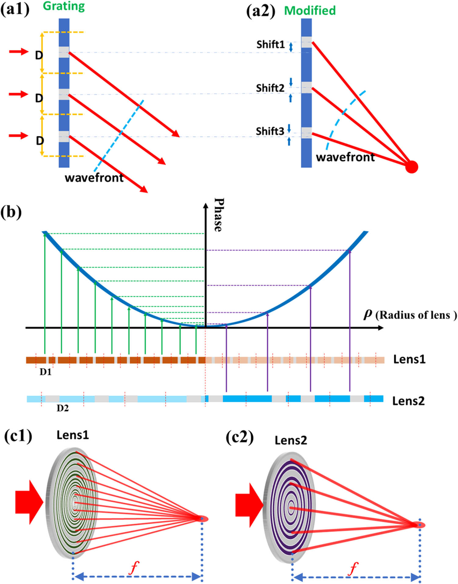
Figure 1.Flexible lens design based on detour phase holography. (a) The principle of detour phase holography. (a1) Each slit in an infinite one-dimensional grating with periodically repeating apertures of period
![]()
Figure 2.Flexible GML fabrication. (a) Schematics for GML fabrication: (a1) a GO film was prepared on the glass substrate, followed by (a2) GML patterning of the GO using a mask-free femtosecond laser direct writing system. (b1)–(b5) Different lens designs with the same focal length, but with linewidths of the annular apertures of 0.5, 1.0, 1.5, 2.0, and 2.5 μm; the total number of annular apertures for these lenses is 74, 37, 23, 18, and 13, respectively. (c1)–(c5) The bright-field microscopic images of the fabricated GMLs corresponding to (b1)–(b5). (d) Optical profiler measurements of the GML in (c3), where the thickness of the GML film is 200 nm.
Figure 1(b) shows the phase distribution along the radial direction of a converging lens. For the discretized paraxial phase profile, different periodicities of the initial grating lead to different aperture locations and thus different lens designs can be obtained. The discretized paraxial phase profile of the converging lens has the following form [42]:
3. EXPERIMENTS AND RESULTS
To prove the effectiveness of the detour phase lens design principle, we designed and fabricated five different lenses based on GO. For all experiments, the working wavelength was 633 nm, the focal length was 300 μm, and the diameter of the lens was 150 μm. To verify the flexibility of our detour phase lens design, the periodicities
The fabrication process includes two steps, as shown in Fig. 2(a): first, coating GO film onto a substrate (cover glass with a refractive index of 1.515); and second, laser patterning of the GML. For the first step, we used the solution-phase layer-by-layer self-assembly method [43], in which the polyelectrolyte polydiallyldimethylammonium chloride (PDDA) and the GO monolayers are coated alternately onto the substrate, leading to a precisely controlled number of layers and film thickness. The thickness of each PDDA–GO bilayer is about 4 nm, so considering the refractive index, a PDDA–GO film with 50 bilayers (200 nm thick) was prepared to obtain a
![]()
Figure 3.Schematic of the experimental setup. A 633 nm collimated He–Ne laser was used as the incident light source. A beam expansion (BE) lens group was used to expand the laser beam to obtain an approximate plane wave. An objective (OBJ) with
![]()
Figure 4.Experimental characterization. (a1)–(a5) Experimental measurements of longitudinal intensity distribution results of GMLs with different linewidths of the ring-shaped aperture ranging from 0.5 to 2.5 μm. (b1)–(b5) The corresponding theoretical focusing intensity distributions of (a1)–(a5). (c1)–(c5) The experimental and calculated cross-sectional intensity distributions on the focal planes of the five GMLs. (d1)–(d5) The experimental and calculated cross-sectional intensity distributions along the optical axis. The lateral sizes of the focal spot show good agreement between the experimental and theoretical results. The maximal deviation of the focusing position is approximately 5 μm, which is about 1.6% of the focal length (300 μm). All intensity values are normalized to the peak value of intensity.
The schematic of the experimental setup for characterizing the focusing property of the GMLs is shown in Fig. 3. A collimated He–Ne laser with illumination wavelength of 633 nm was used as the incident light source; compared with the size of GMLs, this expanded laser beam was an approximate plane wave. The cross-sectional intensity distribution of the focal spots of the GMLs was captured by an
The phase distribution profile of the proposed detour phase lens depends on the shifting distance of the aperture in the periodical structure. Compared with precisely controlling the thickness of the GO to control the desired phase, the shifting distance of the aperture is much easier to achieve with high accuracy positioning stage and no additional processing. We therefore discuss a technique here to precisely control the phase distribution of the focal spots by simply modifying the location of the apertures. The discretized paraxial phase profile of the converging lens should be
![]()
Figure 5.Phase controlling of the focal spot. (a), (b) The intensity and phase distribution of the focusing field for a GML (lens 1) with the focal length of 500 μm. (c), (d) The intensity and phase distribution of the focusing field for another lens (lens 2), which was obtained by adding a uniform phase value to lens 1. The focal spots of lenses 1 and 2 are the same for the intensity distribution, but the phase distributions crossing the focal plane are slightly modified. (e), (f) The phase distributions of lenses 1 and 2 across the focal plane along the optical axis. (g) The corresponding phase values of (e) (blue) and (f) (red). There is a
4. CONCLUSION
We have presented a new implementation of flat diffraction lens design using the detour phase hologram principle, which is based on the aperture shift of periodical structures. Compared with the Fresnel zone plate design, this detour phase lens has demonstrated its high tolerance for designing lenses with the same focal length despite possessing different geometrical structures. This will benefit numerous applications for specializing the design based on specific needs and can significantly relax the fabrication requirements. In the experiment, GMLs were designed and fabricated as examples to verify the proposed method. Good agreement has been found between the experimental and theoretical results. Furthermore, by considering the uniform phase shift in the lens design, the phase distribution of the focal spot could be modified accordingly, with the phase modulation of the focal spot linearly related to the uniform phase shift in the lens design. The detour phase lens design is a promising method that provides optimal high tolerance for a flat diffraction lens design. With less stringent processing requirements, which will reduce the cost of the ultrathin flat lens, this technique will greatly benefit flat lens applications.
Acknowledgment
Acknowledgment. B. J. acknowledges support from the Australia Research Council and the Industrial Transformation Training Centres. X. Y. acknowledges the Natural Science Foundation of Guangdong Province and the Shenzhen Science and Technology Innovation Commission. S. W. acknowledges the National Natural Science Foundation of China, the Foundation of Guangdong Education Committee, and the Foundation of Shenzhen Science and Technology. S. W. and M. S. acknowledge the Shenzhen Science and Technology Innovation Commission. G. C. acknowledges the fellowship of China Postdoctoral Science Foundation.
S. W., H. L., and B. J. conceived the experiment; S. W. and G. C. performed the experiments and prepared the samples. S.W., X. Y., and M. S. prepared the manuscript. All authors discussed and analyzed the results. B. J. supervised the project.
APPENDIX A: GO FILM PREPARATION
We used the layer-by-layer process to prepare the GO film. There are five main steps: (1) GO solution is prepared by using a sonifier cell disruptor with 550 W output, 20 kHz frequency (Branson SFX550); (2) a clean substrate is immersed into a 2.0% (w/v) aqueous PDDA (Sigma-Aldrich) solution for 30 s; (3) the substrate is rinsed with de-ionized water and dried with
APPENDIX B: FEMTOSECOND LASER FABRICATION
A low repetition rate, femtosecond pulsed laser beam (100 fs pulse width, 10 kHz, 800 nm) is used to reduce the GO film through direct laser writing method. By a computer-controlled 3D nanometric piezo stage, 3D arbitrary structures can be created in the sample. The main problem of the GMLs fabrication is to find out the based laser power and speed to ablate the GO film with 0.5 μm linewidth. We used an objective (NA 0.8,
APPENDIX C: ANALYSIS OF ACCEPTABLE PARAMETER RANGE OF THE STRUCTURE
Here, the focusing efficiency of the lens is used as the selection criterion of the lens design parameters. Essentially, different GML designs for the same focusing spot are the different sampling of the convergent wavefront. Sparse sampling may result in insufficient sampling data and affect the lens’s focusing efficiency. As shown in Fig.
![]()
Figure 6.Focusing efficiencies of GMLs at different linewidths. The focusing efficiency changed when the linewidth of the GO structure changed. Both too dense sampling and too sparse sampling processes of the convergent wavefront will reduce the focusing efficiency of the lens. In the green area, the focusing efficiency of the GMLs did not change significantly.
APPENDIX D: THE TABLE OF RING RADII OF THE GMLS
References
[1] Z. Wang, W. Guo, L. Li, B. Luk’yanchuk, A. Khan, Z. Liu, Z. Chen, M. Hong. Optical virtual imaging at 50 nm lateral resolution with a white-light nanoscope. Nat. Commun., 2, 218(2011).
[2] D. Liu, Z. Liu. Hyperlenses and metalenses for far-field super-resolution imaging. Nat. Commun., 3, 1205(2012).
[3] S. W. Hell. Toward fluorescence nanoscopy. Nat. Biotechnol., 21, 1347-1355(2003).
[4] A. I. Barbosa, P. Gehlot, K. Sidapra, A. D. Edwards, N. M. Reis. Portable smartphone quantitation of prostate specific antigen (PSA) in a fluoropolymer microfluidic device. Biosens. Bioelectron., 70, 5-14(2015).
[5] M. M. A. Zeinhom, Y. Wang, Y. Song, M. Zhu, Y. Lin, D. Du. A portable smart-phone device for rapid and sensitive detection of
[6] K. Karakostas, S. Gkagkanis, K. Katsaliaki, P. Köllensperger, A. Hatzopoulos, M. E. Kiziroglou. Portable optical blood scattering sensor. Microelectron. Eng., 217, 111129(2019).
[7] R. Kingslake, R. B. Johnson. Lens Design Fundamentals(2009).
[8] M. Khorasaninejad, W. T. Chen, R. C. Devlin, J. Oh, A. Y. Zhu, F. Capasso. Metalenses at visible wavelengths: diffraction-limited focusing and subwavelength resolution imaging. Science, 352, 1190-1194(2016).
[9] H. Pahlevaninezhad, M. Khorasaninejad, Y. W. Huang, Z. Shi, L. P. Hariri, D. C. Adams, V. Ding, A. Y. Zhu, C. W. Qiu, F. Capasso. Nano-optic endoscope for high-resolution optical coherence tomography
[10] F. Aieta, P. Genevet, M. A. Kats, N. Yu, R. Blanchard, Z. Gaburro, F. Capasso. Aberration-free ultrathin flat lenses and axicons at telecom wavelengths based on plasmonic metasurfaces. Nano Lett., 12, 4932-4936(2012).
[11] N. Yu, F. Capasso. Flat optics with designer metasurfaces. Nat. Mater., 13, 139-150(2014).
[12] S. Shrestha, A. C. Overvig, M. Lu, A. Stein, N. Yu. Broadband achromatic dielectric metalenses. Light Sci. Appl., 7, 85(2018).
[13] B. Xu, H. M. Li, S. L. Gao, X. Hua, C. Yang, C. Chen, F. Yan, S. N. Zhu, T. Li. Metalens-integrated compact imaging devices for wide-field microscopy. Adv. Photonics, 2, 066004(2020).
[14] V. J. Einck, M. Torfeh, A. McClung, D. E. Jung, M. Mansouree, A. Arbabi, J. J. Watkins. Scalable nanoimprint lithography process for manufacturing visible metasurfaces composed of high aspect ratio TiO2 meta-atoms. ACS Photonics, 8, 2400-2409(2021).
[15] Z. X. Shen, S. H. Zhou, X. N. Li, S. J. Ge, P. Chen, W. Hu, Y. Q. Lu. Liquid crystal integrated metalens with tunable chromatic aberration. Adv. Photonics, 2, 036002(2020).
[16] Y. Aharonov, F. Colombo, I. Sabadini, D. Struppa, J. Tollaksen. Some mathematical properties of superoscillations. J. Phys. A, 44, 365304(2011).
[17] Y. Eliezer, L. Hareli, L. Lobachinsky, S. Froim, A. Bahabad. Breaking the temporal resolution limit by superoscillating optical beats. Phys. Rev. Lett., 119, 043903(2017).
[18] G. Yuan, E. T. Rogers, N. I. Zheludev. “Plasmonics” in free space: observation of giant wavevectors, vortices, and energy backflow in superoscillatory optical fields. Light Sci. Appl., 8, 2(2019).
[19] Y.-X. Shen, Y.-G. Peng, F. Cai, K. Huang, D.-G. Zhao, C.-W. Qiu, H. Zheng, X.-F. Zhu. Ultrasonic super-oscillation wave-packets with an acoustic meta-lens. Nat. Commun., 10, 1(2019).
[20] X. Zheng, B. Jia, H. Lin, L. Qiu, D. Li, M. Gu. Highly efficient and ultra-broadband graphene oxide ultrathin lenses with three-dimensional subwavelength focusing. Nat. Commun., 6, 8433(2015).
[21] G. Cao, X. Gan, H. Lin, B. Jia. An accurate design of graphene oxide ultrathin flat lens based on Rayleigh-Sommerfeld theory. Opto-Electron. Adv., 1, 18001201(2018).
[22] G. Cao, H. Lin, S. Fraser, X. Zheng, B. Del Rosal, Z. Gan, S. Wei, X. Gan, B. Jia. Resilient graphene ultrathin flat lens in aerospace, chemical, and biological harsh environments. ACS Appl. Mater. Interfaces, 11, 20298-20303(2019).
[23] H. Lin, S. Fraser, M. H. Hong, M. Chhowalla, D. Li, B. H. Jia. Near-perfect microlenses based on graphene microbubbles. Adv. Photonics, 2, 055001(2020).
[24] X. Li, S. Wei, G. Cao, H. Lin, Y. Zhao, B. Jia. Graphene metalens for particle nanotracking. Photonics Res., 8, 1316-1322(2020).
[25] S. Wei, G. Cao, H. Lin, X. Yuan, M. Somekh, B. Jia. A varifocal graphene metalens for broadband zoom imaging covering the entire visible region. ACS Nano, 15, 4769-4776(2021).
[26] P. Ding, Y. Li, L. Shao, X. Tian, J. Wang, C. Fan. Graphene aperture-based metalens for dynamic focusing of terahertz waves. Opt. Express, 26, 28038-28050(2018).
[27] K.-T. Lin, H. Lin, T. Yang, B. Jia. Structured graphene metamaterial selective absorbers for high efficiency and omnidirectional solar thermal energy conversion. Nat. Commun., 11, 1389(2020).
[28] H. Lin, B. C. Sturmberg, K.-T. Lin, Y. Yang, X. Zheng, T. K. Chong, C. Martijn de Sterke, B. Jia. A 90-nm-thick graphene metamaterial for strong and extremely broadband absorption of unpolarized light. Nat. Photonics, 13, 270-276(2019).
[29] D. Hu, X. Wang, S. Feng, J. Ye, W. Sun, Q. Kan, P. J. Klar, Y. Zhang. Ultrathin terahertz planar elements. Adv. Opt. Mater., 1, 186-191(2013).
[30] M. Khorasaninejad, Z. Shi, A. Y. Zhu, W.-T. Chen, V. Sanjeev, A. Zaidi, F. Capasso. Achromatic metalens over 60 nm bandwidth in the visible and metalens with reverse chromatic dispersion. Nano Lett., 17, 1819-1824(2017).
[31] M. J. Simpson, A. G. Michette. Imaging properties of modified Fresnel zone plates. Optica Acta, 31, 403-413(1984).
[32] K. Miyamoto. The phase Fresnel lens. J. Opt. Soc. Am., 51, 17-20(1961).
[33] H. Arsenault. Diffraction theory of Fresnel zone plates. J. Opt. Soc. Am., 58, 1536(1968).
[34] B. R. Brown, A. W. Lohmann. Complex spatial filtering with binary masks. Appl. Opt., 5, 967-969(1966).
[35] A. W. Lohmann, D. P. Paris. Binary Fraunhofer holograms, generated by computer. Appl. Opt., 6, 1739-1748(1967).
[36] B. R. Brown, A. W. Lohmann. Computer-generated binary holograms. IBM J. Res. Dev., 13, 160-168(1969).
[37] J. P. Hugonin, P. Chavel. A complement to the theory of Lohmann-type computer holograms. Opt. Commun., 16, 342-346(1976).
[38] T.-C. Poon. Digital Holography and Three-Dimensional Display: Principles and Applications(2006).
[39] C. Min, J. Liu, T. Lei, G. Si, Z. Xie, J. Lin, L. Du, X. Yuan. Plasmonic nano‐slits assisted polarization selective detour phase meta‐hologram. Laser Photonics Rev., 10, 978-985(2016).
[40] J. Lin, P. Genevet, M. A. Kats, N. Antoniou, F. Capasso. Nanostructured holograms for broadband manipulation of vector beams. Nano Lett., 13, 4269-4274(2013).
[41] Z. Xie, T. Lei, G. Si, X. Wang, J. Lin, C. Min, X. Yuan. Meta-holograms with full parameter control of wavefront over a 1000 nm bandwidth. ACS Photonics, 4, 2158-2164(2017).
[42] J. W. Goodman. Introduction to Fourier Optics(2005).
[43] Y. Yang, H. Lin, B. Zhang, Y. Zhang, X. Zheng, A. Yu, M. Hong, B. Jia. Graphene-based multilayered metamaterials with phototunable architecture for on-chip photonic devices. ACS Photonics, 6, 1033-1040(2019).
[44] A. Sajjad, O. Hemmatyar, H. Taghinejad, A. Krasnok, Y. Kiarashinejad, M. Zandehshahvar, A. Alù, A. Adibi. Tunable nanophotonics enabled by chalcogenide phase-change materials. Nanophotonics, 9, 1189-1241(2020).
[45] H. Liu, W. Dong, H. Wang, L. Lu, Q. Ruan, Y. Tan, R. E. Simpson, J. K. Yang. Rewritable color nanoprints in antimony trisulfide films. Sci. Adv., 6, eabb7171(2020).
[46] O. Hemmatyar, S. Abdollahramezani, I. Zeimpekis, S. Lepeshov, A. Krasnok, A. I. Khan, K. M. Neilson, C. Teichrib, T. Brown, E. Pop, D. W. Hewark. Enhanced meta-displays using advanced phase-change materials(2021).
[47] M. Y. Shalaginov, S. An, Y. Zhang, F. Yang, P. Su, V. Liberman, J. B. Chou, C. M. Roberts, M. Kang, C. Rios, Q. Du. Reconfigurable all-dielectric metalens with diffraction-limited performance. Nat. Commun., 12, 1225(2021).
[48] M. A. Neil, R. Juškaitis, T. Wilson. Method of obtaining optical sectioning by using structured light in a conventional microscope. Opt. Lett., 22, 1905-1907(1997).
[49] K. Wicker, O. Mandula, G. Best, R. Fiolka, R. Heintzmann. Phase optimisation for structured illumination microscopy. Opt. Express, 21, 2032-2049(2013).


Set citation alerts for the article
Please enter your email address

© Copyright 2018-2021 | Chinese Laser Press. All Rights Reserved 沪ICP备15018463号-20