• Acta Photonica Sinica
  • Vol. 50, Issue 1, 156 (2021)
Lujie WU1、3, Qingtao WEN1、3, Yazeng GAO1、2、5, Weier LU1、2、5, Yang XIA1、2、5, Yanli LI4, Xiangdong KONG2、4, and Li HAN2、4
Author Affiliations
  • 1Instrument and Equipment R&D Center, Institute of Microelectronics, Chinese Academy of Sciences, Beijing00029, China
  • 2University of Chinese Academy of Sciences, Beijing101407, China
  • 3School of Science, Beijing Jiaotong University, Beijing100044, China
  • 4Institute of Electrical Engineering, Chinese Academy of Sciences, Beijing100080, China
  • 5Beijing Engineering Research Center for Microelectronics Preparation Equipment, Beijing100029, China
  • show less
    DOI: 10.3788/gzxb20215001.0123001 Cite this Article
    Lujie WU, Qingtao WEN, Yazeng GAO, Weier LU, Yang XIA, Yanli LI, Xiangdong KONG, Li HAN. Investigation on the Preparation of High Precision Multilayer X-ray Fresnel Zone Plates Based on Atomic Layer Deposition Technology[J]. Acta Photonica Sinica, 2021, 50(1): 156 Copy Citation Text show less
    Schematic diagrams of the FZP structure and imaging optical path
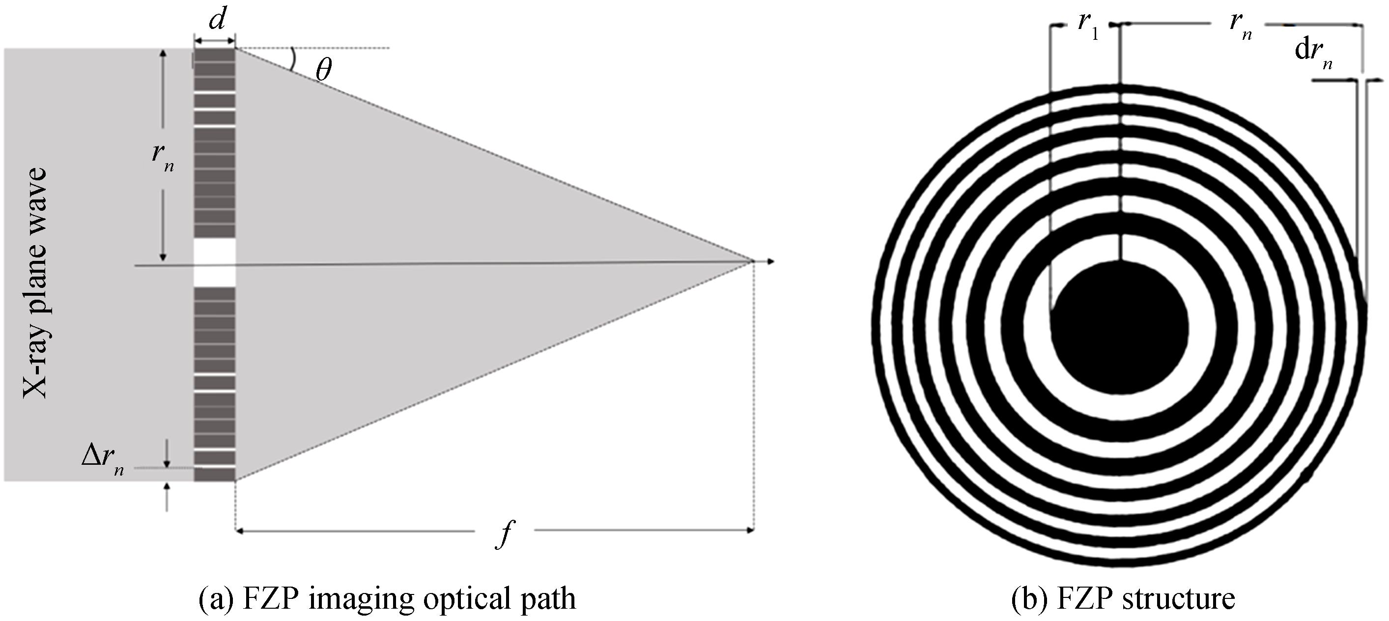
    Fig. 1. Schematic diagrams of the FZP structure and imaging optical path
    The diffraction efficiency calculation of the FZP at the X-ray energy of 8 keV and 15 keV according to coupled wave theory
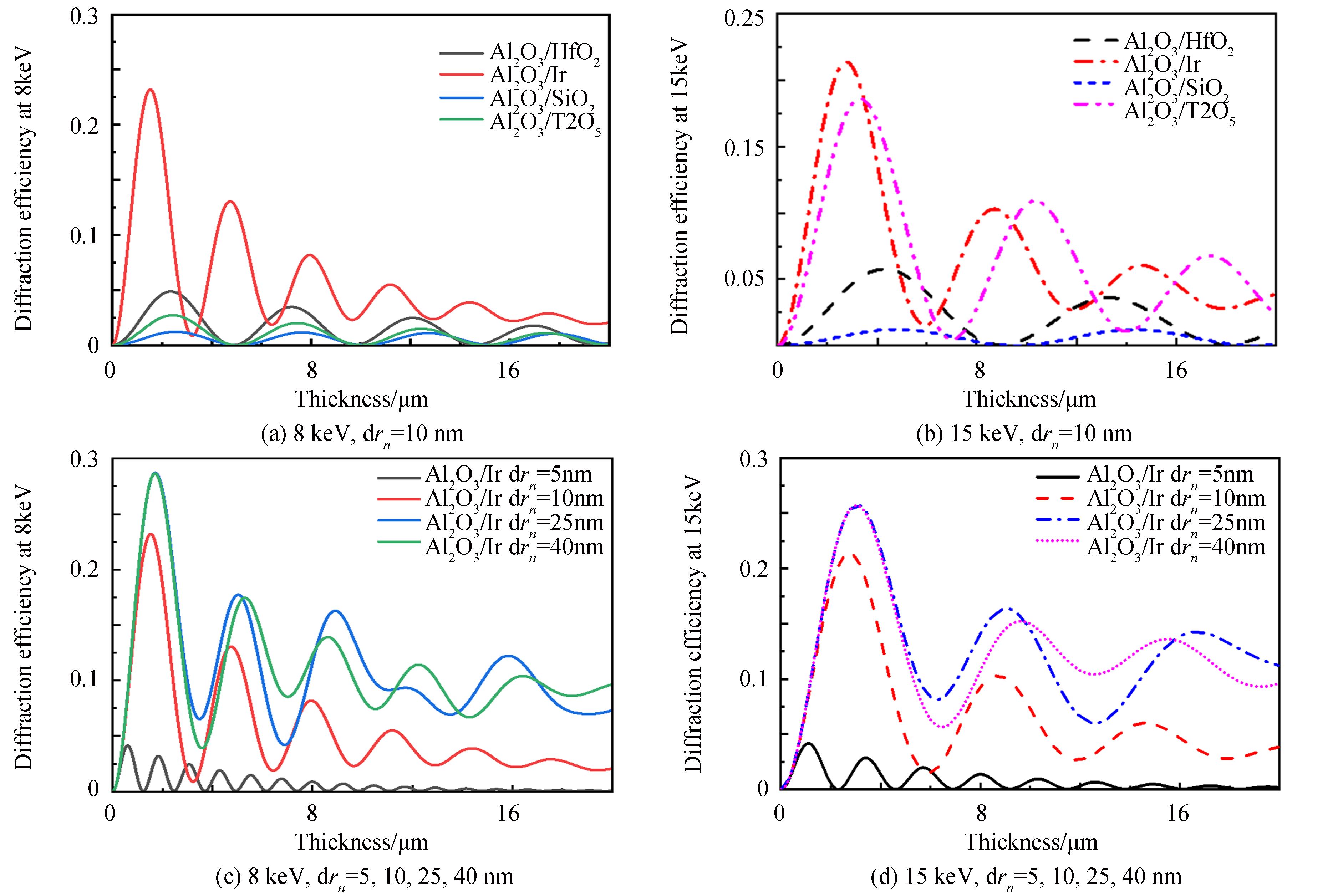
    Fig. 2. The diffraction efficiency calculation of the FZP at the X-ray energy of 8 keV and 15 keV according to coupled wave theory
    Schematic diagram of the source and purging time of Al2O3 and HfO2 films grown by atomic layer deposition
    Fig. 3. Schematic diagram of the source and purging time of Al2O3 and HfO2 films grown by atomic layer deposition
    Schematic diagram of the prepartion structure of the new type of FZP
    Fig. 4. Schematic diagram of the prepartion structure of the new type of FZP
    Al2O3 and HfO2 thin film thicknesses measured through ellipsometer (0.1 nm)
    Fig. 5. Al2O3 and HfO2 thin film thicknesses measured through ellipsometer (0.1 nm)
    SEM and AFM images of the surface morphology of Al2O3 and HfO2 films
    Fig. 6. SEM and AFM images of the surface morphology of Al2O3 and HfO2 films
    The cross-sectional SEM images of 10 nm Al2O3/HfO2 multilayer film (light gray: Al2O3, dark gray: HfO2) prepared by atomic layer deposition technique
    Fig. 7. The cross-sectional SEM images of 10 nm Al2O3/HfO2 multilayer film (light gray: Al2O3, dark gray: HfO2) prepared by atomic layer deposition technique
    SEM images of Al2O3/HfO2 multilayer FZP after focused ion beam cutting and polishing
    Fig. 8. SEM images of Al2O3/HfO2 multilayer FZP after focused ion beam cutting and polishing
    ED/µmd/µmΔr/nmt/µmArf/mmn
    8 keV40301022002.58438
    Table 1. Structural parameters of the FZP with 10 nm outermost zone width at 8 keV
    ERing radius/µmBand width/nmRing radius/µmBand width/nm
    8 keVr563=15.004 85dr563=13.320 00r997=19.967 63dr997=10.011 49
    r564=15.018 17dr564=13.308 2r998=19.977 64dr998=10.006 48
    r565=15.031 48dr565=13.296 43r999=19.987 65dr999=10.001 4
    r566=15.044 78dr566=13.284 69r1000=19.997 65dr1000=9.996 5
    r567=15.058 06dr567=13.272 98r1001=20.007 65dr1001=9.991 48
    Table 2. Zone parameters of the FZP with focal distance of 2.564 mm at 8 keV
    Lujie WU, Qingtao WEN, Yazeng GAO, Weier LU, Yang XIA, Yanli LI, Xiangdong KONG, Li HAN. Investigation on the Preparation of High Precision Multilayer X-ray Fresnel Zone Plates Based on Atomic Layer Deposition Technology[J]. Acta Photonica Sinica, 2021, 50(1): 156
    Download Citation