
Long Wen, Xianghong Nan, Jiaxiang Li, David R. S. Cumming, Xin Hu, Qin Chen. Broad-band spatial light modulation with dual epsilon-near-zero modes[J]. Opto-Electronic Advances, 2022, 5(6): 200093
- Opto-Electronic Advances
- Vol. 5, Issue 6, 200093 (2022)
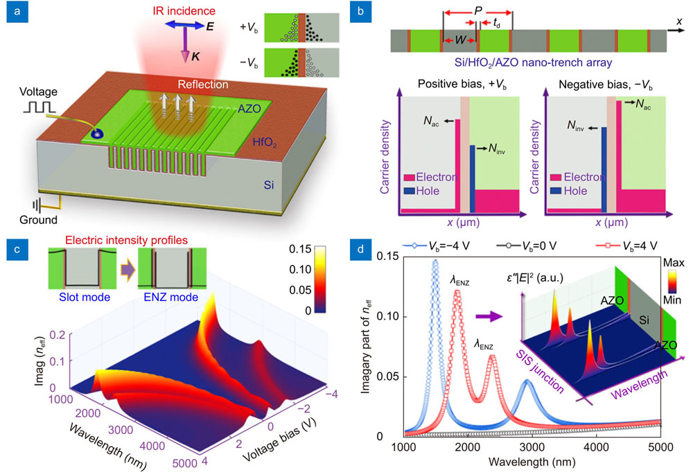
Fig. 1. (a –b ) The schematic drawing of the deep nanotech-based SIS capacitor for broad-band spectral E-O modulation. Under external voltage biasing, the capacitor encounters charge accumulation at both sides of the SIS junction. With a sufficiently high carrier density, dual ENZ confinements can be anticipatedin the nanometer thin layers which results insubstantial E-O absorption along the sidewall of the nanotrench. Herein, the period of the nanotrench (P) is 300 nm, the width of the silicon wall is a half of the period (W=P/2), and the thickness of HfO2 (td) is assumed to be 8 nm. The background doping level of AZO and silicon is 2×10¹⁸ and 2×1017 cm−3, respectively. (c ) The evolution of the mode loss characteristics in the SIS nanotrenchas a function of wavelength and voltage bias. The upper plot shows two typical mode field profiles associated to with and without a voltage bias. (d ) The imaginary part of the effective mode index (neff) plotted at three selected voltages (i.e., Vb=−4, 0 and 4 V). The inset is Pabs of the eigenmodes plotted in the spatial and spectral domains, which illustrates the localized energy absorption properties of the two distinct ENZ modes (Vb= 4 V).
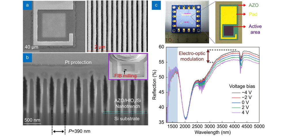
Fig. 2. (a ) Top view SEM images of the deepnanotrenchSIS capacitor. (b ) Side view SEM image of the inner structure of the SIS nanotrenchesafter a section in the central region was milled by FIB.The etched nanowalls were slightly tapered, with the top and bottom widths ranging from 110 to 185 nm and the depthestimated to be 1.3 μm. (c ) The photograph of fabricated device mounted on PCB (left) and the enlarged optical microscopy image of the device area. (d ) The FTIR measured reflection spectra at various voltages.
Fig. 3. (a ) The measured and fitted SE data of the planar reference structure with different incidence angles. The complete structure represented in SE model as a multilayered system (Inset of the top plot). (b ) Optical constants of the PLD deposited AZO film based on the SE fitting. The derived values for the Drude model parameters are: high frequency permittivity ε∞=3.806, carrier density N0=3.3×1020 cm−3 and damping rate γ=1.39 ×10¹⁴ s−1. Based on the SE model, the thickness of the AZO film and HfO2 is found to be 343 and 10 nm, respectively. (c ) Spectral fitting results of the nanostrench and the planar reference devices. The thick and thin curves represent the experimental and fitted results, respectively. Note that, the non-polarization response of nanotrench device is averaged by two orthogonal linear polarizations.
Fig. 4. (a ) The experimental measured high frequency C-V curves of the nanotrench and planar SIS capacitor (open symbols). The result of the planar reference was fitted very well with our electrical model (red line). (b ) Voltage bias-dependent carrier profiles near the SIS junction area obtained from the TCAD modeling using the derived electrical parameters. (c ) The imaginary part of the effective index of the fundamental mode supported by the SIS nanotrench. In the PDE calculations, the spatially varied optical constants of the SIS junction were extrapolated by the Drude model using the carrier profiles shown in (b). (d ) The Pabs distribution across the SIS junction at a wavelength of 3800 nm representing the ENZ modes modulated by voltage biasing.
Fig. 5. Transient E-O response of the AZO/HfO2/p-Si capacitor to applied switching voltage. (a ) Quasistatic-state band diagram of the SIS junction with and without an external voltage bias (left and middle plots). The evolution of carrier distribution near the SIS junction for the capacitor applied with gradually decreased voltages (right plot). (b –c ) Transient carrier and E-O modulation of the proposed SIS capacitor. The E-O modulation property is calculated based on an optical model using the same geometry as that of Fig. 2 (i.e., AZO fully wrapped the nanotrench structure where the depth of the nanotrench is 1.5 μm. For the sake of reducing series resistance, the thickness of substrate is assumed to be 100 μm).

Set citation alerts for the article
Please enter your email address
© Copyright 2018-2021 | Chinese Laser Press. All Rights Reserved 沪ICP备15018463号-20