Abstract
Epsilon-near-zero (ENZ) modes have attracted extensive interests due to its ultrasmall mode volume resulting in extremely strong light-matter interaction (LMI) for active optoelectronic devices. The ENZ modes can be electrically toggled between on and off states with a classic metal-insulator-semiconductor (MIS) configuration and therefore allow access to electro-absorption (E-A) modulation. Relying on the quantum confinement of charge-carriers in the doped semiconductor, the fundamental limitation of achieving high modulation efficiency with MIS junction is that only a nanometer-thin ENZ confinement layer can contribute to the strength of E-A. Further, for the ENZ based spatial light modulation, the requirement of resonant coupling inevitably leads to small absolute modulation depth and limited spectral bandwidth as restricted by the properties of the plasmonic or high-Q resonance systems. In this paper, we proposed and demonstrated a dual-ENZ mode scheme for spatial light modulation with a TCOs/dielectric/silicon nanotrench configuration for the first time. Such a SIS junction can build up two distinct ENZ layers arising from the induced charge-carriers of opposite polarities adjacent to both faces of the dielectric layer. The non-resonant and low-loss deep nanotrench framework allows the free space light to be modulated efficiently via interaction of dual ENZ modes in an elongated manner. Our theoretical and experimental studies reveal that the dual ENZ mode scheme in the SIS configuration leverages the large modulation depth, extended spectral bandwidth together with high speed switching, thus holding great promise for achieving electrically addressed spatial light modulation in near- to mid-infrared regions. Epsilon-near-zero (ENZ) modes have attracted extensive interests due to its ultrasmall mode volume resulting in extremely strong light-matter interaction (LMI) for active optoelectronic devices. The ENZ modes can be electrically toggled between on and off states with a classic metal-insulator-semiconductor (MIS) configuration and therefore allow access to electro-absorption (E-A) modulation. Relying on the quantum confinement of charge-carriers in the doped semiconductor, the fundamental limitation of achieving high modulation efficiency with MIS junction is that only a nanometer-thin ENZ confinement layer can contribute to the strength of E-A. Further, for the ENZ based spatial light modulation, the requirement of resonant coupling inevitably leads to small absolute modulation depth and limited spectral bandwidth as restricted by the properties of the plasmonic or high-Q resonance systems. In this paper, we proposed and demonstrated a dual-ENZ mode scheme for spatial light modulation with a TCOs/dielectric/silicon nanotrench configuration for the first time. Such a SIS junction can build up two distinct ENZ layers arising from the induced charge-carriers of opposite polarities adjacent to both faces of the dielectric layer. The non-resonant and low-loss deep nanotrench framework allows the free space light to be modulated efficiently via interaction of dual ENZ modes in an elongated manner. Our theoretical and experimental studies reveal that the dual ENZ mode scheme in the SIS configuration leverages the large modulation depth, extended spectral bandwidth together with high speed switching, thus holding great promise for achieving electrically addressed spatial light modulation in near- to mid-infrared regions.Introduction
Active controlling the characteristics of the optical signal in amplitude, phase or polarization is essential for a broad application in diverse fields such as optical processing, optical interconnects, adaptive optics, image projection, optical sensing etc.1-7. Tremendous efforts have been made in the past decades towards realizing electrically addressed modulation by carrier dispersion, the Pockels, or quantum confined Stark effect8-10. To meet the ever-increasing demands for modern photonic systems, advanced modulation solutions should encompass not only the high speed and efficient operation, but also the low energy consumption and capability of large-scale integration. Therefore, electro-optic (E-O) modulation on the all-silicon or silicon compatible platform has continued to be at the forefront of research in this field11-13. The inherent weak E-O effect of silicon is the major stumbling block to achieve efficient all-silicon modulation. By employing a high-Q (quality factor) resonant configuration, the silicon modulation in the integrated optics domains has been struggled to satisfy large modulation depth and desired high speed simultaneously, however at the expense of limited spectral bandwidth14-17. In contrast, it becomes even more challenging to realize spatial light modulation relying on silicon E-O effect. Nevertheless, several light-matter interaction (LMI) enhancing strategies have been proposed to achieve silicon-based spatial light modulation17-24. For example, the free carrier electro-refraction (E-R) effect of silicon can be greatly enhanced by incorporating plasmonic design into a metal-oxide-seminconductor (MOS) capacitor configuration18-20. However, as the resonant plasmonic structures are always accompanied by serious Ohmic loss, it is hardly possible to achieve large absolute modulation depth. Alternately, the photonic-crystal (PhC) cavity has been implemented in silicon spatial light modulators, where the enhanced E-R serves as a perturbation to the critical coupled high-Q resonance21-24. Despite the improved modulation depth, such a sensitive high-Q system suffers from narrow spectral bandwidth (typically less than 1 nm in the PhC structure21, 22) and intrinsic poor angular tolerance. The silicon compatible platform with hybrid integration of active medium facilitates the utilization of more efficient E-O mechanisms for free space light modulation1, 2, 25-28. For instance, the liquid crystal on silicon (LCoS) is the most mature technology for spatial light manipulation and has been widely used on both the basic researches and practical applications25. Because of the E-O response of the nematic liquid crystal is typically in the millisecond scale, the main limitation of LCoS technique lies on its slow switching speed. Fabry-Perot cavity with embedded multiple quantum well layers (Ge/SiGe or Ⅲ-Ⅴ MQW) have also been used to create spatial light modulators on silicon26-29. The operation spectral bandwidth is also narrow as the band-edge absorption of MQW occurs at a precisely selected wavelength. Moreover, the hybrid integration of MQW/Si requires sophisticated, complex and expensive fabrication techniques such as multi-layer heteroepitaxy or wafer-bonding.
Recently, the epsilon-near-zero (ENZ) effect based on the transparent conducting oxides (TCOs) has emerged as a robust LMI enhancing scheme for all-optical switch, E-O modulation, perfect absorption/thermal emissionand, etc30-33. In particular, the onset and offset of ENZ confinement on nanometer thick carrier accumulation/depletion layer can be dynamically controlled via classic MOS configuration on the silicon platform. This makes the TCO as a compelling choice for hybrid integration on silicon to achieve more efficient E-O modulation for both the waveguide integrated and free-space optics36-43. In most previous literatures, metal or metal-like materials (e.g. ionic liquids) were used as the gate electrodes while TCO served as the ground semiconductor33-36. The E-O response was achieved upon tuning the carrier density of TCO to match or mismatch the ENZ condition. In other scenarios where silicon is used as the gate electrode36-38, 44, 45, it is should be recalled that an electrostatic potential across the capacitor can also induce carrier accumulation, depletion and inversion in the gate semiconductor. However, those previous studies have normally considered TCO as the sole active medium but seldom explored the carrier dispersion effect in the silicon gate, which may hinder the possible contributions of the E-O or even ENZ responses from silicon. In this work, we demonstrate that broad spectral bandwidth modulation can be achieved in a TCOs/insulator/silicon nanotrench configuration due to the coexistence of ENZ confinements in both thesilicon and TCO. The nanotrench array with a high aspect ratio resembles a vertically aligned waveguide system with low optical loss in the absence of external voltage biasing across the junction. Dual ENZ modes form alongside the nanotrench sidewall when applying a voltage bias, because of the surface carrier accumulation at the both sides of the junction. These highly confined modes propagate in an elongated manner leading to very efficient electro-absorption. Compared to the plasmonic resonance strategy40-43, the non-resonant and metal-less configuration allows for more efficient spatial light modulation with large absolute modulation depth and broad-band spectral operation from near- to mid-infrared. Moreover, to the best of our knowledge, this study presents the first evidence of such a novel phenomenon that the ENZ-based electro-absorption effect can be achieved in silicon and applicable for spatial light modulation.
Dual ENZ-mode for broad-band E-O modulation
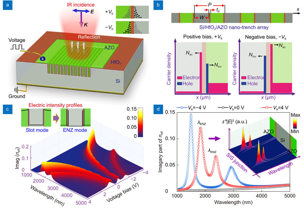
As illustrated in Fig. 1(a), the proposed spatial light modulation scheme is based on a semiconductor-insulator-semiconductor (SIS) nano-capacitor, in which a high aspect ratio Si nanotrench with an ultra-thin conformal coating of high k insulator (HfO2) is assumed to be completely wrapped by Al-doped ZnO (AZO). Both the AZO and silicon are assumed to be n-type semiconductors which have moderate background doping level (N0) to guarantee low optical loss in the IR regime. Imagining from a parallel plate capacitor (inset of Fig. 1(a)), equal and opposite surface charges (Qs) induced by an external voltage bias (Vb) is given by Qs=Cs×Vb, where Cs is area capacitance. To outline the basic modulation principle of the proposed SIS nanotrench capacitor, we first consider a simplified electrical model36, 37 where the accumulation (inversion) layer of electrons (holes) within the semiconductors is in close proximity to the insulator with a constant thickness of ts~1 nm (estimated by the Thomas-Fermi screening length). The carrier distributions in the SIS capacitor with a sufficient voltage bias (assuming Vb=0 is the flat-band voltage), therefore, can be described as (Fig. 1(b)): Nac=Qs/ts+N0, the electron concentration of the accumulation layer for one side; Ninv=Qs/ts−N0, the hole concentration of the inversion layer for the other side. In the IR regime, the complex permittivities of both silicon and AZO are concentration-dependent and can be well approximated by the free carrier model (i.e. Drude model) according to the early reports (see Supplementary information S1). With a sufficiently high carrier density, the crossover wavelength (i.e. ENZ point) of the surface carriers can be continuously modulated in a broad IR wavelength regime for the concentrationlevels related to the varying voltage bias (Vb) in the range of –4 to 4 V (
Fig. S1).

Figure 1.(a–b) The schematic drawing of the deep nanotech-based SIS capacitor for broad-band spectral E-O modulation. Under external voltage biasing, the capacitor encounters charge accumulation at both sides of the SIS junction. With a sufficiently high carrier density, dual ENZ confinements can be anticipatedin the nanometer thin layers which results insubstantial E-O absorption along the sidewall of the nanotrench. Herein, the period of the nanotrench (P) is 300 nm, the width of the silicon wall is a half of the period (W=P/2), and the thickness of HfO2 (td) is assumed to be 8 nm. The background doping level of AZO and silicon is 2×10¹⁸ and 2×1017 cm−3, respectively. (c) The evolution of the mode loss characteristics in the SIS nanotrenchas a function of wavelength and voltage bias. The upper plot shows two typical mode field profiles associated to with and without a voltage bias. (d) The imaginary part of the effective mode index (neff) plotted at three selected voltages (i.e., Vb=−4, 0 and 4 V). The inset is Pabs of the eigenmodes plotted in the spatial and spectral domains, which illustrates the localized energy absorption properties of the two distinct ENZ modes (Vb= 4 V).
Note that, the Si/HfO2/AZO nanotrench array is periodically arranged with a subwavelength pitch (Pλ) in the lateral direction while the depth keeps relatively long for the light propagation direction. Such a subwavelength nano-system allows for non-resonant and near perfect coupling with the free space incidence, and can be considered as a homogeneous medium with its optical properties described by the effective mode index according to the effective-medium theory (EMT)46. We therefore adopted the finite-difference eigenmode (FDE) solver to calculate the mode properties of the SIS nanotrench at different voltages (see Supplementary information S2 for more details). As shown in Fig. 1(c), for the case absent of any external voltage bias, the SIS capacitor in a flat-band condition exhibits a slot mode like feature of the electromagnetic field distribution which gives rise to lossless characteristic throughout a broad IR wavelength regime (1.5–5 μm). In contrast, when applying a voltage across the capacitor, high carrier density layers presented in both the AZO and silicon significantly alters the light propagation/absorption properties at the ENZ points as the IR light trends to couple with the ENZ modes. The resulting E-A efficiency represented by the imaginary part of mode effective index (keff) is illustrated in Fig. 1(c). There are two lossy bands with the peak positions coinciding with the ENZ points of AZO or silicon surface layers, which can be continuously tuned from NIR to MIR regions. Although the densities of surface carriers in the accumulation and inversion layers are close to each other at a given voltage bias, butthe high-frequency permittivity term in the Drude model for silicon is much larger than that for AZO (Supplementary information S1). This fact results in two distinct ENZ wavelengths for the biased capacitor where the silicon related ENZ mode always presents at the longer wavelength, as clearly verified by the spectral distribution of the normalized power density of the eigenmode absorption (inset of Fig. 1(d), defined as
). Considering a reflective-type device architecture (Figure 1(a)) where the IR light passing through the effective medium twice, the modulation depth can be approximated by the Beer’s law: Md=1−e−2α(λ)D, where α and D are the absorption coefficient (4πkeff/λ) and the thickness of the active medium (i.e., the depth of nanotrench). For a positive bias of 4 V, the dual ENZ modulation bands (λ=1830 and 2375 nm) shown in Fig. 1(d) can lead to a Md up to 90% and 60% respectively with a nanotrench depth of 1.5 μm. The nanotrench system based spatial light modulation with an elongated LMI path allows a larger absolute modulation depth as compared to previous plasmonic resonance-ENZ coupling strategies (typically theMd is less than 20%)41-43.
Experimental results of the broad-band E-O modulation
The experimental demonstration of above dual-ENZ modes mediated broadband modulation scheme was also carried out. The silicon nanotrench array with a pitch of 400 nm was defined via e-beam lithography and deep silicon etching process. The gate dielectric HfO2 with a target thickness of 10 nm was prepared by atom layer deposition. To ensure the growth of AZO in a well encapsulated manner, pulse laser deposition (PLD) was used instead of the common sputtering method. The high temperature PLD facilitates the migration ability of adsorbed atoms on substrate and thus can offer high ability of lateral growth on the nanostructures with high aspect ratio, as confirmed in the Supplementary information S3. UV lithography combined with wet etching processes were carried out to leave a small rectangle area of AZO. Subsequently, the front anode electrode with an opening was defined on the AZO mesa. The opening is slightly larger than the area of nanotrench array (60×60 μm2), which allows us to evaluate the modulation property of the SIS capacitor for the reflection beam. Low resistive Ti/Au contact on the rear side of silicon substrate was considered as the ground. Fig. 2(a–b) shows the top-down and side-view SEM images of the fabricated capacitor. The thin layer of AZO can be clearly observed at the sidewalls of the nanotrenches in the Focus Ion Beam (FIB) sample (Fig. 2(b)). Note that, the relatively thick capping layer atop of the nanotrench also points to a preferential orientation growth tendency. This fact can be evidenced by the X-ray diffraction results (see Supplementary information S3), in which the strong (002) diffraction peak with a very narrow FWHM confirms a good quality and high c-axis orientated crystalline structure of the PLD prepared AZO.
Figure 2.(a) Top view SEM images of the deepnanotrenchSIS capacitor. (b) Side view SEM image of the inner structure of the SIS nanotrenchesafter a section in the central region was milled by FIB.The etched nanowalls were slightly tapered, with the top and bottom widths ranging from 110 to 185 nm and the depthestimated to be 1.3 μm. (c) The photograph of fabricated device mounted on PCB (left) and the enlarged optical microscopy image of the device area. (d) The FTIR measured reflection spectra at various voltages.
The completed capacitors were mounted and wire-bonded to pads on a printed circuit board (Fig. 2(c), the upper plots). Focusing upon the dual-ENZ confinement mechanism, the E-O modulation property of the nanotrench SIS capacitor was examined in quasistatic measurements. The reflection spectrum was acquired using a microscope Fourier Transform Infrared Spectrometer (FTIR, Nicolet iN10), in which non-polarized beam can be tuned to match the active area of nanotrench capacitor. Fig. 2(c) shows the measured reflection spectra at various biasing voltages. The reflection spectra was collected over a broad wavenumber range (8000 to 2000 cm–1) but the short-wavelength part (marked as the shadow) of the spectrum becomes very noisy. For all the measured spectra, a shape and large reflection dip located at the wavelength of 2021 nm and a small dip at 2650 nm were observed. These features originate from the ENZ absorption or ray destructive interference, which will be validated later. At longer wavelengths, relative high reflection amplitudes were observed. By imposing different biasing voltages, repeatable variations of the reflection can be clearly observed in our measurements. As revealed in Fig. 2(c), the broadband E-O modulation behavior has been validated qualitatively regarding on the tunable reflection spectra over 2500 nm to 5000 nm. Nevertheless, we are aware of discrepancies when comparing with our previous theoretical results. Apparently, the demonstrated E-O modulation depth (Md~3%) is much smaller than that of the theoretical expectations from Fig. 1(d). The Md can be doubled by employing linear-polarized light modulation scheme, as the ENZ modes can only be excited by incidence that is tangentially polarized to the SIS interface plane. Another important discrepancy related to the experimental data is the monotonous increase of the E-A when tuning the bias from a negative gate voltage to a positive one, whereas the theoretical model suggests onset of the E-A at both positive and negative biasing conditions (refer to Fig. 1(d)). This fact can be properly attributed to the large negative shifts of the electrical neutrality of the experimental devices.
To fully understand above experimental findings, more detailed optical and electrical investigations are needed. Fig. 3(a) shows the Infrared Spectroscopic Ellipsometry (IR-SE) data of the planar AZO/HfO2/silicon structure prepared using the same procedure as the nanotrench capacitor. The measurement was conducted in the spectral range of 300–1680 nm at three angles of incidence (60°, 65°, and 70°). For the wavelengths larger than 1100 nm, the backside reflection passing through the transparent silicon substrate is incoherent with reflections from the top surface. This results in depolarization of the measurement beam as shown in the Fig. 3(a). Therefore, the optical model for the SE fitting should include the depolarization data. The optical constants the ITO layers were analyzed based on the Drude model. The fitting targets are the film thicknesses (roughness layer, AZO layer and HfO2) and the Drude model’s parameters (free carrier density, high frequency permittivity, and damping term). In Fig. 3(a), it is found that the measured depolarization, Psi and Delta data can be fitted very well with our optical model. The carrier concentration of AZO obtained herein is 3.3×1020 cm–3. Based upon the derived Drude model’s parameters, in Fig. 3(b), the complex permittivity of the as-prepared AZO can be extrapolated towards a wide spectrum. The ENZ wavelength (λENZ) represented by the crossover point of real part is found to be around 2000 nm and the corresponding imaginary part is smaller than one. Now, we can adopt the complex permittivity of AZO to mimic the optical property of the nanotrench and planar reference SIS capacitor via FDTD simulation. Most of the geometric parameters (e.g. nanotrench depth, width, thickness of HfO2 and general morphology of AZO coating) used in the FDTD model can be directly measured from the SEM images (Fig. 2(a–b)) or roughly estimated from the beforehand calibrated fabrication process. Although the band bending effect may already exist in the static-state SIS capacitor, we neglect the surface carrier accumulation for the sake of simplicity. Therefore, both the AZO and silicon are assumed to be homogenous with intrinsic carrier related permittivity. As shown in Fig. 3(c), the main spectral features of the measured reflection for both the nanotrench and planar structure can be captured by our optical models (Supplementary information S4). In order to obtain a good match to the dominant reflection dip at 2020 nm, the background doping level of AZO in our nanotrench structure is calibrated to 3.1×1020 cm−3. The slightly lowered carrier concentration can be attributed to the difference in the growth kinetics of the AZO deposited on the nanostructured and planar substrates. For the nanotrench case, the observed shape dip can now be safely ascribed to the ENZ absorption of the thin AZO shell. Regarding to the high background carrier level of AZO, the E-A response from the thin surface charge layer can differ significantly from the situations we consider in Fig. 1. In addition, there is an air gap between the fabricated nanotrenches. The continuity of the electric displacement at the interfaces gives the boundary conditions as: ε1E1=ε2E2. In the wavelengths of 3~5 μm, the unity permittivity of the air gap could be smaller than that of the ENZ layers (εENZ equals the imaginary part of the materials’ permittivity at the ENZ point). The electric field tends to be localized in the air gap area rather than the ENZ layer. Therefore, the existence of the air gap in the fabricated structures could be an important issue leading to the unsatisfactory modulation performance.
Figure 3.(a) The measured and fitted SE data of the planar reference structure with different incidence angles. The complete structure represented in SE model as a multilayered system (Inset of the top plot). (b) Optical constants of the PLD deposited AZO film based on the SE fitting. The derived values for the Drude model parameters are: high frequency permittivity ε∞=3.806, carrier density N0=3.3×1020 cm−3 and damping rate γ=1.39 ×10¹⁴ s−1. Based on the SE model, the thickness of the AZO film and HfO2 is found to be 343 and 10 nm, respectively. (c) Spectral fitting results of the nanostrench and the planar reference devices. The thick and thin curves represent the experimental and fitted results, respectively. Note that, the non-polarization response of nanotrench device is averaged by two orthogonal linear polarizations.
We have previously posed a conjecture that unanticipated monotonous voltage-dependent E-O modulation property encountered in our experiments is related to the electrical neutrality shifts of the SIS capacitor. To demonstrate this, further studies concerning the realistic carrier tuning behavior under external voltage biasing should be carried out, for which we resort to the capacitance-voltage (C-V) measurements on the nano-capacitor and a planar reference (Fig. 4(a)). The two capacitors in comparison share similar C-V profiles at the given biasing voltages. Since the prepared AZO holds a sufficient high background carrier density which cannot be fully depleted at the given positive Vb, the observed high frequency C-V curves are very similar to a typical MOS capacitor. Upon a biasing voltage of Vb~4 V, considering the 3D wraparound junction of the nanotrench scenario, its capacitance per unit area is at least five-times larger than the planar capacitor. Small-signal AC device simulation with previous developed quantum model was also performed to fit the C-V profile of the planar capacitor (see Supplementary information S5 for more details). The trapped-state density on the order of 1012 cm−2 at the silicon/HfO2 interface is found to be crucial for acquisition of the stretch-out property of the C-V curve. Moreover, regarding to the fact that the AZO has an electron affinity close to the silicon (4.05 eV), the large negative shifted C-V curve in measurement indicates the existence of the fixed charges at the interface. Thus, we have taken into account the above mentioned issues via implanting of the interface model (Supplementary information S6, Table 2). Fig. 4(a) shows that the experimental C-V profiles can be accurately fitted by the small-signal AC simulation. The derived carrier density of AZO is around 3.2×1020 cm−3, which appears to be in reasonably good accord with the SE fitted value. According to our simulation, a large negative VFb value of −1.27 V is determined, confirming the shifted electrical neutrality of the SIS capacitor.
Figure 4.(a) The experimental measured high frequency C-V curves of the nanotrench and planar SIS capacitor (open symbols). The result of the planar reference was fitted very well with our electrical model (red line). (b) Voltage bias-dependent carrier profiles near the SIS junction area obtained from the TCAD modeling using the derived electrical parameters. (c) The imaginary part of the effective index of the fundamental mode supported by the SIS nanotrench. In the PDE calculations, the spatially varied optical constants of the SIS junction were extrapolated by the Drude model using the carrier profiles shown in (b). (d) The Pabs distribution across the SIS junction at a wavelength of 3800 nm representing the ENZ modes modulated by voltage biasing.
The theoretical E-O modulation presented in Fig. 1 is based on the assumption that the local change of the surface carrier in semiconductors occurs in a constant thin layer. However, the actual profiles of the surface charge can differ significantly, which have to resort to the solution of the Poisson’s equation for the SIS capacitor under electrostatic potential. Moreover, recent studies found that it is crucial to include the quantum effect beyond the classical device physics for fully understanding of the performance of ENZ modulation in practice39, 42. To this end, to acquire more realistic carrier distributions, we perform the detailed device simulations of the SIS capacitor with the density gradient (D-G) quantum model (Supplementary information S6). Most electrical parameters used in our simulation are based upon the fitting results from the above SE and C-V studies. As shown in Fig. 4(b), with a negative bias of −4 V, the AZO side is in electron accumulation state while the silicon undergoes inversion that accompanied with a moderate high density of holes. For the zero bias case, surface depletion occurs in AZO and only a small amount of electron can be witnessed in silicon. At a positive bias of 4 V, the surface of AZO is forced into a deep depletion mode as inferred by the enlarged space-charge region. It is also notable that a high density of electron is accumulated at the surface of silicon. For revealing the corresponding E-A characters of the SIS capacitor, further optical mode analysis was performed by taking account of spatial carrier dispersion based on the above carrier profiles and the Drude model. Note that, the Drude model for AZO is modified according to the SE fitting results. The fundamental modes supported by the nanotrench capacitor under different voltages were calculated separately and the distribution of keff and Pabs are plotted in Fig. 4(c–d). The keff in a wavelength regime of 2500–5000 nm increases with the increasing voltage bias, which is closely consistent with our experimental observation (Fig. 2(c)). The corresponding E-A modulation can be qualitatively explained from the Pabs distributions along with the carrier profiles shown in Fig. 4(b). At a negative bias of −4 V, the surface accumulation layer in AZO has a peak electron density slightly higher than the background doping level. Its ENZ confinement effect might be almost submerged by the large background ENZ absorption related to the rest neutral region of AZO, resulting in a very limited increment of the mode loss at a short wavelength regime of 1500–2000 nm. Although the inversion hole was observed at the silicon surface, its carrier density is still not high enough for an ENZ permittivity in a mid-IR range (refer to Pabs plot). For the zero bias condition, the electron density of the surface depletion layer in AZO isgradually decreases into a lower carrier density towards the interface. This gives rise to an ENZ confinement at a mid-IR wavelength as confirmed by the Pabs plot (λ=3800 nm, Vb=0). Finally, for the case of positive voltage bias, both the surface electrons in the extended space-charge area of AZO and the accumulation layer of silicon hold a proper carrier profile to allow sufficient ENZ confinements. Dual ENZ confinements in the SIS capacitor can be clearly inferred from the Pabs plot (λ=3800 nm, Vb=4 V), which therefore results in the largest mode loss in the mid-IR range.
Transient analysis of the dual-ENZ E-O modulation
In practice, in addition to the modulation depth and operation wavelength range, another key performance indicator for an E-O modulator is the modulation speed. Although our proof-of-concept experiments were performed at a quasistatic state, its high frequency property can be partially inferred from the small signal C-V measurement. As illustrated in Fig. 4(a), the C-V curves measured at a megahertz frequency are highly asymmetric, suggesting that the fast E-O operation with negative switching voltage will be no longer functional because of the relatively slow carrier generation-recombination processes for the inversion state. Although the prototype design remains valid at positive bias conditions, the high background carrier concentration of AZO has been demonstrated to be unfavorable for mid-IR operation. Paradoxically, if we consider a lightly doped AZO for improving modulation depth, the carrier inversion rather than the partially depletion takes place in AZO for the forward-biased SIS capacitor, which again only allows for low frequency or quasistate E-O modulation. It becomes clear now that, for pursuing high speed and modulation depth, the doping polarity has to be different in the two semiconductors of SIS capacitor. Therefore, the optimum combination for the SIS capacitor is using p-type silicon along with n-type AZO. As shown in the energy band diagram of Fig. 5(a), when applying a negative voltage bias, both silicon and AZO undergo carrier accumulation (hole and electron, respectively). Regarding on the ultra-fast majority carrier transport process, the switching speed of the capacitor is mainly determined by the RC delay time. To confirm this, transient device simulation (Supporting information S6) was carried out to investigate the carrier dynamics induced by the fast switching. The background doping levels in AZO and silicon are assumed to be 2×10¹⁸ and 6×1017 cm−3 respectively, which render the series resistance down to several Ohms and meanwhile low background optical absorption. No interface defect/trap model was included in these calculations as sophisticated surface passivation process can be properly adopted to reduce the surface defect density. The transient carrier response upon a step voltage signal (switch between 0 and −5.5 V) is shown in Fig. 5(b), which suggests that the rise and fall times of the device are 32 ns and 10 ns respectively.
Figure 5.Transient E-O response of the AZO/HfO2/p-Si capacitor to applied switching voltage. (a) Quasistatic-state band diagram of the SIS junction with and without an external voltage bias (left and middle plots). The evolution of carrier distribution near the SIS junction for the capacitor applied with gradually decreased voltages (right plot). (b–c) Transient carrier and E-O modulation of the proposed SIS capacitor. The E-O modulation property is calculated based on an optical model using the same geometry as that of Fig. 2 (i.e., AZO fully wrapped the nanotrench structure where the depth of the nanotrench is 1.5 μm. For the sake of reducing series resistance, the thickness of substrate is assumed to be 100 μm).
Based on the Drude model, the calculated transient carrier profiles from electrical simulation were then incorporated to extrapolate the spatially varied material’s permittivity in the nanotrench SIS junction. The whole capacitor structure in the scope of EMT can be described as the simple multilayer system where the nanotrench layer is considered as a homogenous film with effective refraction index obtained from the 1D eigenmode calculation. Note that, to eliminate the unwanted intensive interference fringes in the calculated spectra, the thick substrate (e.g. 300 μm) was assumed to be a complete incoherent medium (for further details of the models, see Supplementary information S7). Based upon this semi-analytical approach, the changes of the reflectance of the capacitor at different time points can be obtained. The resulting transient and broad-band spectral modulation is given in Fig. 5(c). At the saturated state, the relative modulation depths are found to be 72% and 40% for the two dominate wavelengths associated with surface carrier induced ENZ confinements (i.e. 2030 nm and 3410 nm). Meanwhile, the proposed SIS device shows a switch speed less than 50 ns, thereby holding great promise for high speed spatial light modulation.
Conclusions
In summary, we proposed a broad-band spectral modulation scheme for spatial light by using electrically addressed dual ENZ confinements in a deep nanotrench-based SIS capacitor. While the free carrier electro-refraction effect in silicon is frequently used in E-O modulators, our results highlight the possibility to utilize electro-absorption effect in silicon through similar ENZ confinement scheme as the TCO materials. Based upon the TCO/HfO2/silicon configuration, the field-effect induced surface charge layers adjacent to both sides of the SIS junction can lead to two lossy and well-confined ENZ modesthat contribute to substantial and broad-band light absorption along sidewalls of the deep trench. The broad-band E-O modulation characteristics of the SIS capacitor operated at steady-state were thoroughly analyzed and confirmed by theoretical and experimental studies. We demonstrated that the proposed E-O scheme with proper device optimization allows for high speed operation and large absolute modulation depth around 40–70% for a broad wavelength range between NIR and MIR. Utilizing the dual ENZ confinement effect in similar TCO/silicon-based SIS structures holds great potential to enable broad-band and high-speed spatial light modulation on the fully integrated silicon platform.
References
[1] Efron U, Liverscu G. Multiple quantum well spatial light modulators. Spatial Light Modulator Technology: Materials, Devices and Applications, Efron U, Eds. ; Dekker: New York (1995).
[24] O'brien BB, Burns BE, Hu KL, Ionescu AC. Silicon spatial light modulator. US Pat, 5170283, 1992.
[25] Lazarev G, Hermerschmidt A, Krüger S, Osten S. LCOS spatial light modulators: trends and applications. Optical Imaging and Metrology (Eds Osten W, Reingand N), John Wiley & Sons (2012).