
Yuansheng Tao, Haowen Shu, Xingjun Wang, Ming Jin, Zihan Tao, Fenghe Yang, Jingbo Shi, Jun Qin, "Hybrid-integrated high-performance microwave photonic filter with switchable response," Photonics Res. 9, 1569 (2021)
- Photonics Research
- Vol. 9, Issue 8, 1569 (2021)
Abstract
1. INTRODUCTION
Microwave filters are indispensable building blocks in radio frequency (RF) receivers and are paramount to myriad applications, including radar, wireless communication, and sensing [1–3]. Due to the electronic bottleneck, traditional electronic microwave filters are facing significant challenges for meeting the exponentially increasing capacity in next-generation RF systems [4,5]. For instance, 6G wireless networks in the near future are expected to support an ultrahigh data transmission rate of 100 Gb/s in which the higher RF spectrum region such as mm wave (30 to 300 GHz) shall be harnessed [6,7], while the valid operation frequency of existing electronic filters is commonly restricted below 10 GHz [8]. As a promising alternative, microwave photonic filters (MPFs), which perform filtering operations in the optical domain, are capable of offering wideband tunability along with high stability, low latency, and strong immunity to electromagnetic interference [9]. Such outstanding advantages have propelled abundant explorations on MPFs over the past decades [10–14]. Nevertheless, conventional MPFs are implemented based on bulk devices or benchtop instruments and hence are plagued by the limitations in system cost, space, and power consumption.
Recently, the integration of MPF systems onto a chip-scale platform has been driven by advances in nanophotonic fabrication techniques, which is termed “integrated MPFs” [5]. Considerable progress has been made on integrated MPFs that explore different schemes based on microring resonators (MRRs) [15,16], Mach–Zehnder interferometers (MZIs) [17], waveguide Bragg gratings [18], microcombs [19,20], on-chip stimulated Brillouin scattering [21,22], etc. These demonstrations prove the inherent superiorities of integrated MPFs, in terms of compact footprint, light weight, and scalability. However, in most reported integrated MPFs, only the passive components are incorporated on chip, while all necessary active devices, including lasers, modulators, and photodetectors (PDs), are off-chip and based on fiber connections. The overall systems of such integrated MPFs are still complex, with high power dissipation and sensitivity to environmental fluctuations, thus imposing restrictions on their deployments in real RF systems. Therefore, a higher degree of photonic integration is becoming an urgent pursuit for the implementation of integrated MPFs.
To date, few attempts to create an MPF in high photonic integration have been executed based on monolithic platforms, including indium phosphorus (InP) and silicon platforms. The InP platform can enable monolithic integration of all necessary active and passive devices, on which the first fully integrated MPF was realized [23]. However, issues related to large propagation loss severely limit the accessible spectral resolution on this platform (e.g., 3 dB bandwidth is 2.5 to 5.5 GHz in Ref. [23]). Compared with the InP platform, the silicon photonics platform offers moderately low loss, together with small size, high-volume production, and compatibility with electronic circuits [24]. More recently, MPFs in a high integration level based on a silicon platform have also been demonstrated [25,26]. For example, a silicon highly integrated bandpass MPF consisting of a phase modulator, a micro-disk resonator, and a PD was reported; this MPF features a passband bandwidth of 1.93 GHz, a frequency tunable range within 3 to 10 GHz, and an extinction ratio of 15 dB [25]. Nevertheless, a chip-scale laser source has always been absent for silicon-integrated MPFs due to an indirect bandgap.
Sign up for Photonics Research TOC. Get the latest issue of Photonics Research delivered right to you!Sign up now
Despite these achievements, several pivotal problems still persist, hindering the follow-up development of integrated MPFs. First, the realized filtering performances as indicated above are relatively limited and not competitive with those of discrete MPFs. Generally, toward next-generation RF applications, the integrated MPF is supposed to meet rigorous filtering characteristics, including a sub-GHz bandwidth [4], large rejection ratio (
In this work, we address all the aforementioned points and demonstrate an all-integrated high-performance MPF. This integrated MPF is realized through hybrid integration of an InP chip-scale laser and a monolithic silicon chip consisting of a dual-drive Mach–Zehnder modulator (DDMZM), a high-
2. PRINCIPLES AND DESIGN
The architecture of the hybrid integrated MPF is illustrated in Fig. 1(a), incorporating an InP waveguide-integrated distributed feedback (DFB) laser and a monolithic silicon chip onto the submount. The silicon chip consists of three key devices: a DDMZM, a high-
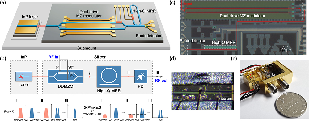
Figure 1.(a) Schematic diagram of the hybrid integrated MPF. (b) The operation principles for the bandpass/band-stop switchable filtering response of the integrated MPF. (c) Optical image of the fabricated silicon chip. (d) Optical image of the InP laser diode chip. (e) Photograph of the packaged hybrid integrated MPF that comprises an InP laser, a silicon chip, and auxiliary microlenses and prism.
The monolithic silicon photonics chip is designed in-house and fabricated on a 220 nm SOI platform leveraging CMOS-compatible processes by Advanced Micro Foundry, as shown in Fig. 1(c). The footprint of the whole chip is about
The integrated light source used here is a commercially available InP DFB laser diode die (
3. EXPERIMENTAL RESULTS
A. Characterization of Key Devices
The transmission spectrum of the high-
![]()
Figure 2.(a) Measured transmission spectrum of the high-
Then, the performances of the active devices in this hybrid integrated MPF were evaluated. The output of the InP-based DFB laser was sent into an optical spectrum analyzer (OSA, Yokogawa 6370C) to characterize the laser spectrum, as seen in Fig. 3(a). The side mode suppression ratio is higher than 55 dB around 1552 nm. The linewidth of the laser was measured by a delayed self-heterodyne (DSH) method (Appendix D), which is extracted as narrow as 150 kHz, as shown in Fig. 3(b). For the DDMZM, the static insertion loss is
![]()
Figure 3.(a) Measured output spectra of the InP-based laser chip under different operation temperatures. (b) DSH linewidth measurement (blue dots) and a Voigt curve fit (red line) show a 3 dB Lorentzian linewidth of 150 kHz.
B. Filtering Response
Using the setup shown in Fig. 4, two experiments for measuring the RF filtering response of the integrated MPF were performed. In the first experiment, the RF spectra were measured based on the monolithic silicon chip and an external light source (EXFO, T100S-HP). In this case, a CW light was generated by the external laser and injected into the silicon chip with a power of
![]()
Figure 4.Experimental setup to measure the band-stop/bandpass filtering response of the integrated MPF.
The frequency response of the integrated MPF operating as a band-stop filter was measured first. A resonance notch at 1552.27 nm was selected to filter the upper sideband of the AS-DSB optical signals. Through precisely controlling the DC bias phase of the DDMZM to enable full cancellation of two beat sidebands, a deep RF frequency notch was realized at
![]()
Figure 5.(a) Measured RF responses of the band-stop filtering at various center frequencies. (b) 3 dB bandwidths and rejection ratios are plotted versus RF frequencies.
Next, the integrated MPF operating as a bandpass filter was demonstrated and evaluated. By setting
![]()
Figure 6.(a) Measured RF responses of the bandpass filtering at different center frequencies. (b) 3 dB bandwidths and rejection ratios are plotted versus RF frequencies.
In the second experiment, the filtering response was evaluated and validated experimentally based on the hybrid all-integrated MPF with package. That is, the InP chip-based laser was turned on, and the microwave signals were input/output of the packaged MPF module through the peripheral RF connectors. The other measurement settings remained unchanged compared with those in the first experiment. In this way, evident bandpass filtering and band-stop filtering profiles were also able to be observed, as shown in Fig. 7(a) and Fig. 7(b), respectively. However, the filtering functionalities are only valid across a limited frequency range, and the performance metrics are far worse than those achieved in Figs. 5 and 6. The noise power spectral density was also evaluated at 3 GHz with 2 mA generated photocurrent, which is around
![]()
Figure 7.Experimental results for the hybrid all-integrated MPF with package. (a) Measured RF spectra of the band-stop filtering. (b) Measured RF spectra of the bandpass filtering. (c) Measured
The damaged filtering performances are due to the severe internal RF crosstalk [23], mostly induced by the RF packaging operation. As seen in Fig. 7(c), when the chip-based InP laser is turned off and turned on, the two obtained
Nevertheless, the proposed hybrid integration scheme to realize an all-integrated MPF is practicable. With further improvements in RF packaging and optical coupling, much higher filtering performances can be envisioned. For example, the RF crosstalk can be effectively eliminated by placing the RF pads of DDMZM and PD at opposite chip edges to have larger spatial distance in future tape-out. Based on our current chip layout, to fully exploit the truly entire functionalities of this integrated MPF, the setup of the first experiment was adopted in subsequent measurements.
C. RF Link Performance
In addition to the filtering functionalities, the RF link performance is also an important issue, which should be considered for the integrated MPF, mainly including RF link gain, noise figure, and spurious-free dynamic range (SFDR) [43]. The link gain G is defined as the RF power ratio of the output signal to the input signal, which was measured by a VNA after calibration. For the noise figure (NF), the expression can be given by [5]
![]()
Figure 8.(a) Measured RF link gain and noise figure over the whole tunable frequency range. (b) Measured power of the fundamental (FUND) component and the third-order intermodulation (IMD3) component versus different input RF power.
In order to obtain the SFDR, a standard two-tone test was carried out. Two RF tones at 3 and 3.01 GHz were generated by two analog signal generators (ASGs, Keysight E8257D and Anritsu MG3695A), combined by an RF coupler, and then applied to the DDMZM. The RF tones are located at the passband of the integrated MPF. An ESA was used to study the RF spectrum detected by the on-chip PD. The powers of the fundamental components (FUND, 3 and 3.01 GHz) and the third-order intermodulation components (IMD3, 3.02 and 2.99 GHz) were extracted under different input RF power, as shown in Fig. 8(b). Given a measured noise floor of
D. High-Resolution Switchable RF Filtering
To testify that our proposed integrated MPF holds the capacity to handle practical tasks in real-world RF systems, we performed high-resolution switchable RF filtering of analog signals toward two typical application scenarios. The first scenario is that the received signal of interest is accompanied by a spectrally closed strong interferer. In such case, the integrated MPF should operate as a highly selective notch filter to suppress the interferer for maximizing the signal-to-noise ratio (SNR) [28]. In the demonstration experiment, a targeted signal at 15 GHz and an unwanted interferer at 15.25 GHz were provided by two ASGs and combined by an RF coupler and then act as input of the integrated MPF. After passing through the integrated MPF, the output RF spectrum was measured and analyzed by an ESA. As shown in Fig. 9(a), if the inputs are located away from the filter stopband, the targeted signal has a power of
![]()
Figure 9.High-resolution RF filtering using the integrated MPF as a band-stop filter. The input contains two frequency components (signal at 15 GHz and interferer at 15.25 GHz). (a) Measured RF spectrum when the input is located outside the stopband. (b) Measured RF spectrum when the interferer is filtered by the stop band.
The second scenario is that multiple frequency bands simultaneously exist in RF environments, while each time only one channel signal is supposed to be isolated and processed. Under this situation, a center-frequency tunable bandpass filter is needed to carry out the channel selection [30]. To simulate this real-scene, two RF signals at 11 GHz as channel 1 and at 13 GHz as channel 2 with equal power were generated to serve as input of the integrated MPF. The integrated MPF was switched to the bandpass operation mode by adjusting
![]()
Figure 10.High-resolution RF filtering using the integrated MPF as a bandpass filter. The input contains two channel signals, i.e., channel 1 (CH1, 11 GHz) and channel 2 (CH2, 13 GHz). (a) Measured RF spectrum when the CH1 is located at the passband. (b) Measured RF spectrum when the CH2 is located at the passband.
These results above highlight the advanced filtering performances of the integrated MPF, in combinations of high operation frequency, high-resolution selectivity, and large rejection ratio. Meanwhile, the filtering response is proved to be agilely switched between the band-stop and bandpass for coping with dissimilar type of signals, which is expected to be quite useful for reducing RF system volumes and improving versatility.
4. DISCUSSION
To benchmark the overall performance of the proposed integrated MPF in this work, we make a comparison among state-of-the-art integrated MPFs and electronic microwave filters, as displayed in Table 1. First, we observe that the spectral resolution and suppression ratio achieved in our work are competitive with those of electronic microwave filters, while the frequency tunable range is much broader thanks to the intrinsic advantages of microwave photonics (MWP) technology. Second, for all the integrated MPFs with high integration degree (
Performance Comparison of State-of-the-Art Integrated MPFs and Electronic Microwave Filters
| 3 dB Bandwidth (GHz) | |||||||||
|---|---|---|---|---|---|---|---|---|---|
| Electronic [ | N/A | N/A | Band-stop | 4–6/6.3–11.4 | 0.035/0.306 | N/A | –2 | N/A | |
| Electronic [ | N/A | N/A | Bandpass | 5.07–5.53 | 0.46 | N/A | –1.5 | N/A | |
| Optical filter | 25% | Bandpass | 1–20 | 0.02–0.35 | N/A | –5 | N/A | ||
| Optical filter | 25% | Band-stop | 0–15 | 3 | 96.5 | –10.1 | 27.1 | ||
| InP [ | Optical filter | 25% | Bandpass | 0–27 | 1.9–5.4 | 32 | 86.3 | N/A | 23.2 |
| Optical filter | 25% | Bandpass/Band-stop | 4–25 | 4.54–9.72/3.65–6.35 | N/A | –10 | N/A | ||
| Optical filter | 25% | Band-stop | 0–12 | 0.15–0.35 | 116 | 8 | 15.6 | ||
| SOI [ | Optical filter | 25% | Band-stop | 2–15 | 0.91 | N/A | N/A | N/A | |
| SOI [ | Optical filter | 25% | Bandpass | 2–18.4 | 0.17 | 26.5 | N/A | –42 | N/A |
| SOI [ | Optical filter | 25% | Bandpass | 4–10 | 0.0035 | 70 | 90.3 | –17.3 | 56.7 |
| SOI [ | Optical filter and PD | 50% | Bandpass | 0–25 | 5.3–19.5 | N/A | N/A | N/A | |
| SOI [ | Modulator, optical filter, and PD | 75% | Bandpass | 3–10 | 1.93 | 15 | 92.4 | –38.9 | N/A |
| SOI [ | Modulator, optical filter, and PD | 75% | Bandpass/Band-stop | 9–21/5–25 | N/A | N/A | N/A | N/A | |
| InP | Laser, modulator, optical filter, and PD | 100% | Low-pass | 0–6 | 2.5–5.5 | 30 | 81.4 | –20 | N/A |
| InP + SOI | Laser, modulator, optical filter, and PD | 100% | Bandpass/Band-stop | 3–21/3–25 | 0.36–0.47/0.38–0.45 | 99.7 | –28.2 | 51.2 |
The performance metrics are evaluated experimentally in 75% photonic integration, where the laser, optical filter, and modulator are on-chip and the PD is off-chip.
The performance metrics are evaluated experimentally in 75% photonic integration, where the modulator, optical filter, and PD are on-chip and the laser is off-chip.
Because the achieved filtering performances are capable of coping with the practical tasks, the remaining hurdle is the RF link performance. The lowest RF-to-RF insertion loss of our proposed integrated MPF is 28.2 dB, which is much larger than that of electronic filters. There are two major factors responsible for the RF insertion loss and they are the high optical link loss and the limited E/O and O/E conversion efficiencies. Hence, the RF insertion loss is possible to be greatly decreased if these two issues could be effectively solved. For reducing the optical link loss, the hybrid integration approach by micro-optics adopted in this work can be replaced by a more efficient photonic wire-bonding technique to achieve an ultralow coupling loss of 0.4 dB [35]. The main on-chip insertion loss derived from the silicon MZ modulator can also be reduced through optimization of the doped region in the waveguide to avoid unnecessary free-carrier absorption [50]. Alternatively, chip-based III-V/Si optical amplifiers could be considered for compensating the propagation loss [51]. For improving the efficiencies of E/O and O/E conversion, a highly efficient silicon MZ modulator with a U-shaped PN junction has recently been demonstrated to have a low half-wave voltage of only 1.7 V [52], and a Ge-Si PD based on whispering gallery structure has reached a high responsivity of 1.04 A/W [53]. Furthermore, utilizing the novel cascaded MRR scheme reported in Ref. [54] will also yield an improvement of link gain. In addition to the optimization of optical devices, the RF loss can also be compensated in the electrical domain by placing a low-noise RF amplifier at the input to the modulator.
Additionally, the SFDR of this integrated MPF is limited by the intrinsic nonlinearity of the silicon modulator, which may also need further promotion. Prospects to improve the SFDR of the silicon modulator have been illustrated by linearization approaches [55–57]. For example, via manipulating power distribution of a dual-parallel MZ silicon modulator, the SFDR for IMD3 has been improved to an ultrahigh value of
Looking forward, with recent developments on large-bandwidth (
5. CONCLUSION
In summary, we have demonstrated an all-integrated high-performance MPF with bandpass/band-stop switchable filtering response, through hybrid InP and Si integration. This integrated MPF achieves high filtering performances in combination of a broad frequency tunable range, a narrow 3 dB bandwidth, and a large rejection ratio as well as agile (
Acknowledgment
Acknowledgment. The authors thank Advanced Micro Foundry (AMF) for silicon device fabrication and Shenzhen PhotonX Technology Co., Ltd. for the support on packages.
APPENDIX A: PRINCIPLE OF SWITCHABLE FILTERING
As shown in Fig.
The
Combining Eqs. (
To implement a bandpass filter, the
To implement a band-stop filter, the
APPENDIX B: HYBRID INTEGRATION OF THE InP LASER CHIP AND THE Si CHIP
In the hybrid integration process, the InP laser diode chip and the Si photonic chip were optically connected based on off-the-shelf micro-optics components. Figure
![]()
Figure 11.(a) Beam propagation simulation for the hybrid integration of the InP laser and Si chip utilizing micro-optics. (b) Measured total coupling loss between these two chips. Green line: InP laser output subtracting all link propagation loss except coupling loss. Orange line: optical power measured from the monitor grating located behind the DDMZM.
A package scheme was developed for assembling this entire hybrid photonics system. First, the InP chip was mounted at an AlN ceramic submount, which has high thermal conductivity. Second, the PCB bonded with Si chip was placed at the metal substrate. Third, the microlens and prism were manually positioned and fixed, one by one in the order that light passes through them, as shown in Fig.
In order to evaluate the coupling efficiency between the InP laser and Si chip, the optical spectrum emitted from the monitor grating (1:9, located behind the DDMZM) was received by an OSA (Yokogawa 6370C), which has a power of
APPENDIX C: PHASE RESPONSE MEASUREMENT OF THE HIGH-Q MRR
The phase response of the high-
APPENDIX D: LINEWIDTH MEASUREMENT OF THE InP LASER
The spectral linewidth of the integrated InP laser was characterized by a DSH approach. The laser output was split into two paths through a 3 dB coupler. One path was 80 MHz frequency shifted by an acousto-optic modulator (AOM, Gooch & Housego). The other path was delayed by a 10 km long-haul fiber. The light beams from these two paths were recombined again by another 3 dB coupler and then were injected into a PD (Finisar, XPDV2150R). The recovered electrical signal was detected by an ESA (Keysight 9010B). To verify the effectiveness of the DSH setup, we first independently measured the linewidth of a commercial laser, which is equal to the specified linewidth of 10 kHz.
APPENDIX E: PERFORMANCE DETAILS OF ON-CHIP MODULATOR AND PD
The performances of the on-chip modulator and PD in this integrated MPF were characterized through the preset monitor grating couplers. The EO
![]()
Figure 12.(a) Measured
The free spectral range (FSR) of the asymmetric MZ modulator is
For the PD, the OE
APPENDIX F: LONG-TERM STABILITY OF THE FILTERING PERFORMANCES
To evaluate the long-term stability of the filtering performances, the rejection ratio and 3 dB bandwidth under band-stop filtering function are measured across a 1 h period. A TEC was adopted to stabilize the operation temperature at 23°C. The RF filtering spectra were acquired by a VNA (Keysight N5247A) with a 10 min interval, as shown in Fig.
![]()
Figure 13.(a) Measurement of the band-stop filter rejection ratio over 1 h continuous operation. (b) Measurement of the 3 dB bandwidth over 1 h continuous operation.
APPENDIX G: RESPONSE TIME OF FILTER FUNCTION SWITCHING
The switching operation between the bandpass and band-stop filter function is realized by changing the phase difference of the DDMZM, using the TiN microheater placed on waveguides. As a consequence, the required time for switching operation is determined by the response speed of the TiN microheater. To characterize the transient response of this thermo-optic switching process, a 1 kHz square-wave electrical signal was generated by a function waveform generator (RIGOL, DG2102 250 MSa/s) to drive the microheater. The modulated optical signal was converted to an electrical signal by an InGaAs photodetector (Thorlabs DET08CFC/M) and then was received by a digital oscilloscope (RIGOL, DS7014 10 GSa/s). Figure
![]()
Figure 14.Time-domain measurement of the TiN microheater placed on the DDMZM. (a) Temporal waveform of the applied square-wave electrical signal. (b) Measured temporal response with a rise/fall time of 15 and 48 μs.
References
[1] S. Pan, Y. Zhang. Microwave photonic radars. J. Lightwave Technol., 38, 5450-5484(2020).
[2] C. Liu, J. Wang, L. Cheng, M. Zhu, G.-K. Chang. Key microwave-photonics technologies for next-generation cloud-based radio access networks. J. Lightwave Technol., 32, 3452-3460(2014).
[3] J. Hervás, A. L. Ricchiuti, W. Li, N. H. Zhu, C. R. Fernández-Pousa, S. Sales, M. Li, J. Capmany. Microwave photonics for optical sensors. IEEE J. Sel. Top. Quantum Electron., 23, 327-339(2017).
[4] Y. Xie, Z. Geng, L. Zhuang, M. Burla, C. Taddei, M. Hoekman, A. Leinse, C. G. Roeloffzen, K.-J. Boller, A. J. Lowery. Programmable optical processor chips: toward photonic RF filters with DSP-level flexibility and mHz-band selectivity. Nanophotonics, 7, 421-454(2018).
[5] Y. Liu, A. Choudhary, D. Marpaung, B. J. Eggleton. Integrated microwave photonic filters. Adv. Opt. Photon., 12, 485-555(2020).
[6] S. Dang, O. Amin, B. Shihada, M.-S. Alouini. What should 6G be?. Nat. Electron., 3, 20-29(2020).
[7] B. Zong, C. Fan, X. Wang, X. Duan, B. Wang, J. Wang. 6G technologies: key drivers, core requirements, system architectures, and enabling technologies. IEEE Veh. Technol. Mag., 14, 18-27(2019).
[8] W. Peng, I. Hunter. Electronically tunable filters. IEEE Microw. Mag., 10, 46-54(2009).
[9] J. Capmany, D. Novak. Microwave photonics combines two worlds. Nat. Photonics, 1, 319-330(2007).
[10] J. Yao. Photonics to the rescue: a fresh look at microwave photonic filters. IEEE Microw. Mag., 16, 46-60(2015).
[11] F. Zeng, J. Yao. All-optical bandpass microwave filter based on an electro-optic phase modulator. Opt. Express, 12, 3814-3819(2004).
[12] W. Li, M. Li, J. Yao. A narrow-passband and frequency-tunable microwave photonic filter based on phase-modulation to intensity-modulation conversion using a phase-shifted fiber Bragg grating. IEEE Trans. Microw. Theory Tech., 60, 1287-1296(2012).
[13] W. Zhang, R. A. Minasian. Switchable and tunable microwave photonic Brillouin-based filter. IEEE Photon. J., 4, 1443-1455(2012).
[14] X. Han, J. Yao. Bandstop-to-bandpass microwave photonic filter using a phase-shifted fiber Bragg grating. J. Lightwave Technol., 33, 5133-5139(2015).
[15] M. S. Rasras, K.-Y. Tu, D. M. Gill, Y.-K. Chen, A. E. White, S. S. Patel, A. Pomerene, D. Carothers, J. Beattie, M. Beals, J. Michel, L. C. Kimerling. Demonstration of a tunable microwave-photonic notch filter using low-loss silicon ring resonators. J. Lightwave Technol., 27, 2105-2110(2009).
[16] H. Qiu, F. Zhou, J. Qie, Y. Yao, X. Hu, Y. Zhang, X. Xiao, Y. Yu, J. Dong, X. Zhang. A continuously tunable sub-gigahertz microwave photonic bandpass filter based on an ultra-high-
[17] E. J. Norberg, R. S. Guzzon, J. S. Parker, L. A. Johansson, L. A. Coldren. Programmable photonic microwave filters monolithically integrated in InP–InGaAsP. J. Lightwave Technol., 29, 1611-1619(2011).
[18] M. Burla, L. R. Cortés, M. Li, X. Wang, L. Chrostowski, J. Azaña. Integrated waveguide Bragg gratings for microwave photonics signal processing. Opt. Express, 21, 25120-25147(2013).
[19] X. Xue, Y. Xuan, H.-J. Kim, J. Wang, D. E. Leaird, M. Qi, A. M. Weiner. Programmable single-bandpass photonic RF filter based on Kerr comb from a microring. J. Lightwave Technol., 32, 3557-3565(2014).
[20] X. Xu, M. Tan, J. Wu, T. G. Nguyen, S. T. Chu, B. E. Little, R. Morandotti, A. Mitchell, D. J. Moss. Advanced adaptive photonic RF filters with 80 taps based on an integrated optical micro-comb source. J. Lightwave Technol., 37, 1288-1295(2019).
[21] D. Marpaung, B. Morrison, M. Pagani, R. Pant, D.-Y. Choi, B. Luther-Davies, S. J. Madden, B. J. Eggleton. Low-power, chip-based stimulated Brillouin scattering microwave photonic filter with ultrahigh selectivity. Optica, 2, 76-83(2015).
[22] M. Garrett, Y. Liu, P. Ma, D.-Y. Choi, S. J. Madden, B. J. Eggleton. Low-RF-loss and large-rejection reconfigurable Brillouin-based RF photonic bandpass filter. Opt. Lett., 45, 3705-3708(2020).
[23] J. S. Fandiño, P. Muñoz, D. Doménech, J. Capmany. A monolithic integrated photonic microwave filter. Nat. Photonics, 11, 124-129(2017).
[24] M. H. Idjadi, F. Aflatouni. Nanophotonic phase noise filter in silicon. Nat. Photonics, 14, 234-239(2020).
[25] W. Zhang, J. Yao. On-chip silicon photonic integrated frequency-tunable bandpass microwave photonic filter. Opt. Lett., 43, 3622-3625(2018).
[26] L. Xu, J. Hou, H. Tang, Y. Yu, Y. Yu, X. Shu, X. Zhang. Silicon-on-insulator-based microwave photonic filter with widely adjustable bandwidth. Photon. Res., 7, 110-115(2019).
[27] R. W. Ridgway, C. L. Dohrman, J. A. Conway. Microwave photonics programs at DARPA. J. Lightwave Technol., 32, 3428-3439(2014).
[28] E. J. Naglich, J. Lee, D. Peroulis, W. J. Chappell. A tunable bandpass-to-bandstop reconfigurable filter with independent bandwidths and tunable response shape. IEEE Trans. Microwave Theory Tech., 58, 3770-3779(2010).
[29] J. Lee, E. J. Naglich, H. H. Sigmarsson, D. Peroulis, W. J. Chappell. New bandstop filter circuit topology and its application to design of a bandstop-to-bandpass switchable filter. IEEE Trans. Microwave Theory Tech., 61, 1114-1123(2013).
[30] R. A. Minasian. Ultra-wideband and adaptive photonic signal processing of microwave signals. IEEE J. Quantum Electron., 52, 0600813(2015).
[31] D. Marpaung, J. Yao, J. Capmany. Integrated microwave photonics. Nat. Photonics, 13, 80-90(2019).
[32] J. Kim, S. Aghaeimeibodi, J. Carolan, D. Englund, E. Waks. Hybrid integration methods for on-chip quantum photonics. Optica, 7, 291-308(2020).
[33] Y. Gao, J.-C. Lo, S. Lee, R. Patel, L. Zhu, J. Nee, D. Tsou, R. Carney, J. Sun. High-power, narrow-linewidth, miniaturized silicon photonic tunable laser with accurate frequency control. J. Lightwave Technol., 38, 265-271(2020).
[34] B. Snyder, B. Corbett, P. O’Brien. Hybrid integration of the wavelength-tunable laser with a silicon photonic integrated circuit. J. Lightwave Technol., 31, 3934-3942(2013).
[35] M. R. Billah, M. Blaicher, T. Hoose, P.-I. Dietrich, P. Marin-Palomo, N. Lindenmann, A. Nesic, A. Hofmann, U. Troppenz, M. Moehrle, S. Randel, W. Freude, C. Koos. Hybrid integration of silicon photonics circuits and InP lasers by photonic wire bonding. Optica, 5, 876-883(2018).
[36] M. Blaicher, M. R. Billah, J. Kemal, T. Hoose, P. Marin-Palomo, A. Hofmann, Y. Kutuvantavida, C. Kieninger, P.-I. Dietrich, M. Lauermann, S. Wolf, U. Troppenz, M. Moehrle, F. Merget, S. Skacel, J. Witzens, S. Randel, W. Freude, C. Koos. Hybrid multi-chip assembly of optical communication engines by
[37] A. Novack, M. Streshinsky, T. N. Huynh, T. Galfsky, M. Hochberg. A silicon photonic transceiver and hybrid tunable laser for 64 Gbaud coherent communication. Optical Fiber Communication Conference, Th4D.4(2018).
[38] A. W. Elshaari, W. Pernice, K. Srinivasan, O. Benson, V. Zwiller. Hybrid integrated quantum photonic circuits. Nat. Photonics, 14, 285-298(2020).
[39] D. T. Spencer, T. Drake, T. C. Briles, J. Stone, L. C. Sinclair, C. Fredrick, Q. Li, D. Westly, B. R. Ilic, A. Bluestone. An optical-frequency synthesizer using integrated photonics. Nature, 557, 81-85(2018).
[40] Q. Deng, L. Liu, X. Li, Z. Zhou. Arbitrary-ratio 1 × 2 power splitter based on asymmetric multimode interference. Opt. Lett., 39, 5590-5593(2014).
[41] W. Bogaerts, P. De Heyn, T. Van Vaerenbergh, K. De Vos, S. Kumar Selvaraja, T. Claes, P. Dumon, P. Bienstman, D. Van Thourhout, R. Baets. Silicon microring resonators. Laser Photon. Rev., 6, 47-73(2012).
[42] X. Guo, Y. Liu, T. Yin, B. Morrison, M. Pagani, O. Daulay, W. Bogaerts, B. J. Eggleton, A. Casas-Bedoya, D. Marpaung. Versatile silicon microwave photonic spectral shaper. APL Photon., 6, 036106(2021).
[43] Y. Liu, D. Marpaung, A. Choudhary, J. Hotten, B. J. Eggleton. Link performance optimization of chip-based Si3N4 microwave photonic filters. J. Lightwave Technol., 36, 4361-4370(2018).
[44] E. J. Naglich, A. C. Guyette, D. Peroulis. High-
[45] A. Boutejdar, A. Ibrahim, W. Ali. Design of compact size and tunable band pass filter for WLAN applications. Electron. Lett., 52, 1996-1997(2016).
[46] Y. Liu, A. Choudhary, G. Ren, K. Vu, B. Morrison, A. Casas-Bedoya, T. G. Nguyen, D.-Y. Choi, P. Ma, A. Mitchell, S. J. Madden, D. Marpaung, B. J. Eggleton. Integration of Brillouin and passive circuits for enhanced radio-frequency photonic filtering. APL Photon., 4, 106103(2019).
[47] H. Yang, J. Li, P. Zheng, G. Hu, B. Yun, Y. Cui. A stopband and passband switchable microwave photonic filter based on integrated dual ring coupled Mach-Zehnder interferometer. IEEE Photon. J., 11, 5502608(2019).
[48] Y. Liu, J. Hotten, A. Choudhary, B. J. Eggleton, D. Marpaung. All-optimized integrated RF photonic notch filter. Opt. Lett., 42, 4631-4634(2017).
[49] S. Gertler, E. A. Kittlaus, N. T. Otterstrom, P. T. Rakich. Tunable microwave-photonic filtering with high out-of-band rejection in silicon. APL Photon., 5, 096103(2020).
[50] G. T. Reed, G. Z. Mashanovich, F. Y. Gardes, M. Nedeljkovic, Y. Hu, D. J. Thomson, K. Li, P. R. Wilson, S.-W. Chen, S. S. Hsu. Recent breakthroughs in carrier depletion based silicon optical modulators. Nanophotonics, 3, 229-245(2014).
[51] K. Van Gasse, R. Wang, G. Roelkens. 27 dB gain III–V-on-silicon semiconductor optical amplifier with >17 dBm output power. Opt. Express, 27, 293-302(2019).
[52] G. Zhou, L. Zhou, Y. Guo, S. Chen, L. Lu, L. Liu, J. Chen. 32 Gb/s OOK and 64 Gb/s PAM-4 modulation using a single-drive silicon Mach–Zehnder modulator with 2 V drive voltage. IEEE Photon. J., 11, 6603610(2019).
[53] Z. Su, E. S. Hosseini, E. Timurdogan, J. Sun, M. Moresco, G. Leake, T. N. Adam, D. D. Coolbaugh, M. R. Watts. Whispering gallery germanium-on-silicon photodetector. Opt. Lett., 42, 2878-2881(2017).
[54] Z. Zhu, Y. Liu, M. Merklein, O. Daulay, D. Marpaung, B. J. Eggleton. Positive link gain microwave photonic bandpass filter using Si3N4-ring-enabled sideband filtering and carrier suppression. Opt. Express, 27, 31727-31740(2019).
[55] J. Ding, S. Shao, L. Zhang, X. Fu, L. Yang. Method to improve the linearity of the silicon Mach-Zehnder optical modulator by doping control. Opt. Express, 24, 24641-24648(2016).
[56] Y. Tao, H. Shu, M. Jin, X. Wang, L. Zhou, W. Zou. Numerical investigation of the linearity of graphene-based silicon waveguide modulator. Opt. Express, 27, 9013-9031(2019).
[57] Q. Zhang, H. Yu, P. Xia, Z. Fu, X. Wang, J. Yang. High linearity silicon modulator capable of actively compensating input distortion. Opt. Lett., 45, 3785-3788(2020).
[58] H. Zhang, M. Li, Y. Zhang, D. Zhang, Q. Liao, J. He, S. Hu, B. Zhang, L. Wang, X. Xiao, N. Qi, S. Yu. 800 Gbit/s transmission over 1 km single-mode fiber using a four-channel silicon photonic transmitter. Photon. Res., 8, 1776-1782(2020).
[59] Y. Ding, Z. Cheng, X. Zhu, K. Yvind, J. Dong, M. Galili, H. Hu, N. A. Mortensen, S. Xiao, L. K. Oxenløwe. Ultra-compact integrated graphene plasmonic photodetector with bandwidth above 110 GHz. Nanophotonics, 9, 317-325(2020).
[60] L. Zhang, L. Jie, M. Zhang, Y. Wang, Y. Xie, Y. Shi, D. Dai. Ultrahigh-
[61] T. Hao, Y. Liu, J. Tang, Q. Cen, W. Li, N. Zhu, Y. Dai, J. Capmany, J. Yao, M. Li. Recent advances in optoelectronic oscillators. Adv. Photon., 2, 044001(2020).
[62] L. R. Cortés, D. Onori, H. G. de Chatellus, M. Burla, J. Azaña. Towards on-chip photonic-assisted radio-frequency spectral measurement and monitoring. Optica, 7, 434-447(2020).
[63] Z. Tang, S. Pan, J. Yao. A high resolution optical vector network analyzer based on a wideband and wavelength-tunable optical single-sideband modulator. Opt. Express, 20, 6555-6560(2012).
[64] T.-Y. Liow, K.-W. Ang, Q. Fang, J.-F. Song, Y.-Z. Xiong, M.-B. Yu, G.-Q. Lo, D.-L. Kwong. Silicon modulators and germanium photodetectors on SOI: monolithic integration, compatibility, and performance optimization. IEEE J. Sel. Top. Quantum Electron., 16, 307-315(2009).


Set citation alerts for the article
Please enter your email address

© Copyright 2018-2021 | Chinese Laser Press. All Rights Reserved 沪ICP备15018463号-20