• Photonics Research
  • Vol. 11, Issue 1, 65 (2023)
Dianzhuang Zheng1, Shuiying Xiang1、2、6、*, Xingxing Guo1, Yahui Zhang1, Biling Gu1, Hongji Wang3, Zhenzhen Xu3, Xiaojun Zhu4, Yuechun Shi3、5、7、*, and Yue Hao2
Author Affiliations
  • 1State Key Laboratory of Integrated Service Networks, Xidian University, Xi'an 710071, China
  • 2State Key Discipline Laboratory of Wide Band Gap Semiconductor Technology, School of Microelectronics, Xidian University, Xi'an 710071, China
  • 3Key Laboratory of Intelligent Optical Sensing and Manipulation, Ministry of Education, National Laboratory of Solid State Microstructures, College of Engineering and Applied Sciences, Institute of Optical Communication Engineering, Nanjing University, Nanjing 210023, China
  • 4School of Information Science and Technology, Nantong University, Nantong 226019, China
  • 5Yongjiang Laboratory, Ningbo 315202, China
  • 6e-mail: syxiang@xidian.edu.cn
  • 7e-mail: yuechun-shi@ylab.ac.cn
  • show less
    DOI: 10.1364/PRJ.471950 Cite this Article Set citation alerts
    Dianzhuang Zheng, Shuiying Xiang, Xingxing Guo, Yahui Zhang, Biling Gu, Hongji Wang, Zhenzhen Xu, Xiaojun Zhu, Yuechun Shi, Yue Hao. Experimental demonstration of coherent photonic neural computing based on a Fabry–Perot laser with a saturable absorber[J]. Photonics Research, 2023, 11(1): 65 Copy Citation Text show less
    Schematic diagram of the coherent photonic spiking neural network.
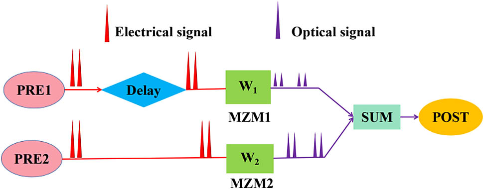
    Fig. 1. Schematic diagram of the coherent photonic spiking neural network.
    (a) Experimental setup for the coherent photonic spiking neural network; (b) integrated FP-SA chip and (c) two input signals Vin1 and Vin2 generated by AWG. AWG, arbitrary waveform generator; Vin1 and Vin2, input signals; TL, tunable laser; DL, delay line; VOA, variable optical attenuator; PC1 and PC2, polarization controller; EA1 and EA2, electronic amplifier; MZM1 and MZM2, Mach–Zehnder modulator; OC, optical coupler; PD, photodetector; PM, powermeter; OSA, optical spectrum analyzer; Bias&T Controller, bias and temperature controller; Scope, oscilloscope. The black (red) lines correspond to optical (electrical) path. The saturable absorber was reversely biased with the voltage source.
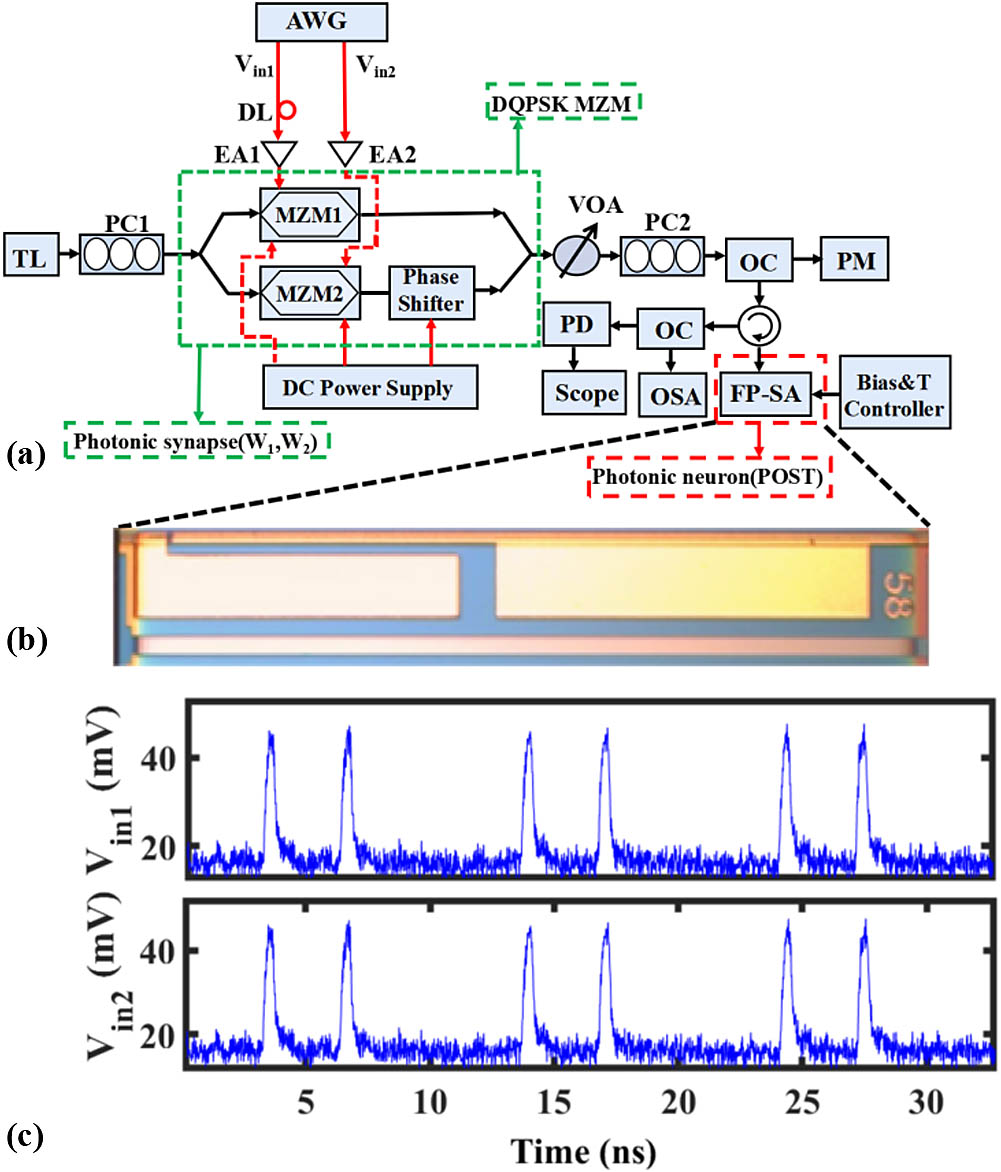
    Fig. 2. (a) Experimental setup for the coherent photonic spiking neural network; (b) integrated FP-SA chip and (c) two input signals Vin1 and Vin2 generated by AWG. AWG, arbitrary waveform generator; Vin1 and Vin2, input signals; TL, tunable laser; DL, delay line; VOA, variable optical attenuator; PC1 and PC2, polarization controller; EA1 and EA2, electronic amplifier; MZM1 and MZM2, Mach–Zehnder modulator; OC, optical coupler; PD, photodetector; PM, powermeter; OSA, optical spectrum analyzer; Bias&T Controller, bias and temperature controller; Scope, oscilloscope. The black (red) lines correspond to optical (electrical) path. The saturable absorber was reversely biased with the voltage source.
    (a) PI curve and (b) optical spectrum of the FP-SA measured at 25°C. The total length of the FP-SA chip is 1500 μm, the width of the laser chip is 300 μm, the ridge waveguide width is 2.5 μm, and the length of the SA region is 75 μm. The SA section side facet and gain section side facet are coated with reflections of 95% and 30%, respectively.
    Fig. 3. (a) PI curve and (b) optical spectrum of the FP-SA measured at 25°C. The total length of the FP-SA chip is 1500 μm, the width of the laser chip is 300 μm, the ridge waveguide width is 2.5 μm, and the length of the SA region is 75 μm. The SA section side facet and gain section side facet are coated with reflections of 95% and 30%, respectively.
    Modulation characteristics of the DQPSK single-drive MZM. The phase shifter is 0. The bias voltage of MZM1 (MZM2) is V1 (V2). (a) V1=4.5 V; (b) V2=4.5 V; (c) V1=V2.
    Fig. 4. Modulation characteristics of the DQPSK single-drive MZM. The phase shifter is 0. The bias voltage of MZM1 (MZM2) is V1(V2). (a) V1=4.5  V; (b) V2=4.5  V; (c) V1=V2.
    Experimental demonstration of temporal integration property and spike threshold property. (a1) and (a2) indicate temporal integration property. (a1) represents the input signals for the weighted summation and (a2) denotes the response of the FP-SA neuron. (b1) and (b2) indicate spike threshold property. (b1) represents the input signals for the weighted summation and (b2) denotes the response of the FP-SA neuron. Temporal maps show the laser neuron’s responses to 100 successive external stimuli, where (c1) corresponds to the stimulus in (a1) and (c2) to the stimulus in (b1). The bias voltage of the FP-SA is −1.846 V, and the bias current is 62.8 mA.
    Fig. 5. Experimental demonstration of temporal integration property and spike threshold property. (a1) and (a2) indicate temporal integration property. (a1) represents the input signals for the weighted summation and (a2) denotes the response of the FP-SA neuron. (b1) and (b2) indicate spike threshold property. (b1) represents the input signals for the weighted summation and (b2) denotes the response of the FP-SA neuron. Temporal maps show the laser neuron’s responses to 100 successive external stimuli, where (c1) corresponds to the stimulus in (a1) and (c2) to the stimulus in (b1). The bias voltage of the FP-SA is 1.846  V, and the bias current is 62.8 mA.
    Experimental demonstration of the refractory period property. (a1) and (a2) indicate that FP-SA neurons are in the refractory period regime. (a1) represents the input signals for the weighted summation and (a2) denotes the response of the FP-SA neuron. (b1) and (b2) indicate that the FP-SA neuron has left the refractory period regime. (b1) represents the input signals for the weighted summation and (b2) denotes the response of the FP-SA neuron. Temporal maps show the laser neuron’s responses to 100 successive external stimuli, where (c1) corresponds to the stimulus in (a1) and (c2) to the stimulus in (b1). The bias voltage of the FP-SA is −1.846 V, and the bias current is 62.8 mA.
    Fig. 6. Experimental demonstration of the refractory period property. (a1) and (a2) indicate that FP-SA neurons are in the refractory period regime. (a1) represents the input signals for the weighted summation and (a2) denotes the response of the FP-SA neuron. (b1) and (b2) indicate that the FP-SA neuron has left the refractory period regime. (b1) represents the input signals for the weighted summation and (b2) denotes the response of the FP-SA neuron. Temporal maps show the laser neuron’s responses to 100 successive external stimuli, where (c1) corresponds to the stimulus in (a1) and (c2) to the stimulus in (b1). The bias voltage of the FP-SA is 1.846  V, and the bias current is 62.8 mA.
    Experimental demonstration of the effect of frequency detuning on spike threshold property. (a) represents the input stimulus signal. (b1)–(b3) denote the response of the FP-SA neuron, corresponding to the three optical spectra for the FP-SA that operates as a photonic spiking neuron, as shown in (c1)–(c3). The bias voltage of the FP-SA is −1.846 V, and the bias current is 62.8 mA.
    Fig. 7. Experimental demonstration of the effect of frequency detuning on spike threshold property. (a) represents the input stimulus signal. (b1)–(b3) denote the response of the FP-SA neuron, corresponding to the three optical spectra for the FP-SA that operates as a photonic spiking neuron, as shown in (c1)–(c3). The bias voltage of the FP-SA is 1.846  V, and the bias current is 62.8 mA.
    Spike response of the FP-SA neuron when injecting the triangular stimulus signal. (a) represents the input signal where the light intensity varies as a triangular wave. (b1) and (b2) denote the response of the FP-SA neuron. (c) represents the ISI interval distribution corresponding to the first type of spike and the second type of spike. The bias voltage of the FP-SA is −1.846 V, and the bias current is 62.8 mA.
    Fig. 8. Spike response of the FP-SA neuron when injecting the triangular stimulus signal. (a) represents the input signal where the light intensity varies as a triangular wave. (b1) and (b2) denote the response of the FP-SA neuron. (c) represents the ISI interval distribution corresponding to the first type of spike and the second type of spike. The bias voltage of the FP-SA is 1.846  V, and the bias current is 62.8 mA.
    V1(V)W1V2(V)W2
    3.0013.001
    5.620.85.400.8
    6.910.66.800.6
    8.210.47.900.4
    9.500.29.300.2
    11.36011.000
    Table 1. Weight Corresponding to the Voltage
    Dianzhuang Zheng, Shuiying Xiang, Xingxing Guo, Yahui Zhang, Biling Gu, Hongji Wang, Zhenzhen Xu, Xiaojun Zhu, Yuechun Shi, Yue Hao. Experimental demonstration of coherent photonic neural computing based on a Fabry–Perot laser with a saturable absorber[J]. Photonics Research, 2023, 11(1): 65
    Download Citation