• Acta Photonica Sinica
  • Vol. 51, Issue 11, 1104002 (2022)
Qian WANG, Jiangtao XU*, Zhiyuan GAO, and Quanmin CHEN
Author Affiliations
  • Tianjin Key Laboratory of Imaging and Sensing Microelectronics,School of Microelectronics,Tianjin University,Tianjin 300072,China
  • show less
    DOI: 10.3788/gzxb20225111.1104002 Cite this Article
    Qian WANG, Jiangtao XU, Zhiyuan GAO, Quanmin CHEN. Effect of Transfer Gate Doping on Full Well Capacity and Dark Current in CMOS Active Pixels[J]. Acta Photonica Sinica, 2022, 51(11): 1104002 Copy Citation Text show less
    4T-PPD pixel structure profile of P+ TG and N+ TG
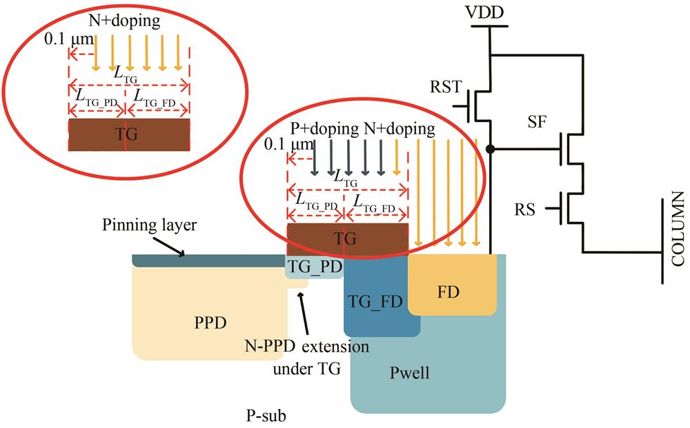
    Fig. 1. 4T-PPD pixel structure profile of P+ TG and N+ TG
    Potential diagram along the emission current path of P+ TG and N+ TG
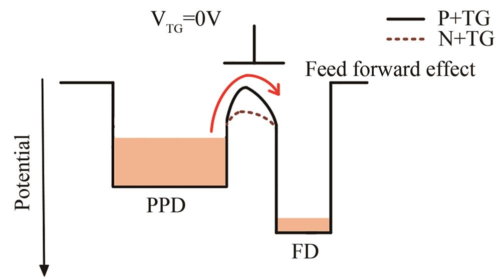
    Fig. 2. Potential diagram along the emission current path of P+ TG and N+ TG
    Two-dimensional simulation profiles
    Fig. 3. Two-dimensional simulation profiles
    One-dimensional potential diagrams under TG
    Fig. 4. One-dimensional potential diagrams under TG
    Simulation results of FWC and dark charges with two types of doped TG at 0 V
    Fig. 5. Simulation results of FWC and dark charges with two types of doped TG at 0 V
    Simulation results of FWC and dark current with two types of doped TG at various VTG_off
    Fig. 6. Simulation results of FWC and dark current with two types of doped TG at various VTG_off
    Simulation results of CTE with P+TG and N+TG
    Fig. 7. Simulation results of CTE with P+TG and N+TG
    One-dimensional potential diagram under TG channels with TG on
    Fig. 8. One-dimensional potential diagram under TG channels with TG on
    ParameterValueUnit
    Absolute temperature,T300K
    Silicon forbidden bandgap, Eg1.12eV
    Boltzmann constant,K1.38×10-23J/K
    Doping concentration in channel region of substrate,Na1.5×1017cm-3
    Intrinsic carrier concentration,ni1.5×1010cm-3
    Thickness of oxide layer,d6nm
    Width of TG,W1μm
    Length of TG,L0.6μm
    Dielectric constant,εo8.85×10-12F/m
    Relative dielectric constant of the silicon,εs11.9-
    Relative dielectric constant of the oxide layer,εr3.9-
    Table 1. The design parameters in this paper
    Qian WANG, Jiangtao XU, Zhiyuan GAO, Quanmin CHEN. Effect of Transfer Gate Doping on Full Well Capacity and Dark Current in CMOS Active Pixels[J]. Acta Photonica Sinica, 2022, 51(11): 1104002
    Download Citation