Henry C. Frankis1,*, Hamidu M. Mbonde1, Dawson B. Bonneville1, Chenglin Zhang1..., Richard Mateman2, Arne Leinse2 and Jonathan D. B. Bradley1|Show fewer author(s)
Abstract
We demonstrate 5 dB net gain in an erbium-doped tellurium-oxide-coated silicon nitride waveguide. The amplifier design leverages the high refractive index and high gain in erbium-doped tellurite glass as well as the ultra-low losses and mature, reliable, and low-cost fabrication methods of silicon nitride waveguide technology. We show that the waveguide platform demonstrates low background propagation losses of 0.25 dB/cm based on a ring resonator device with a factor of at 1640 nm. We measure 5 dB peak net gain at 1558 nm and of net gain across the C band in a 6.7 cm long waveguide for 35 mW of launched 1470 nm pump power. Gain per unit length of 1.7 and 1.4 dB/cm is measured in a 2.2 cm long waveguide for 970 and 1470 nm pump wavelengths, respectively. Amplifier simulations predict that gain can be achieved across the C band simply by optimizing waveguide length and fiber-chip coupling. These results demonstrate a promising approach for the monolithic integration of compact erbium-doped waveguide amplifiers on silicon nitride chips and within silicon-based photonic integrated circuits.1. INTRODUCTION
Silicon nitride () photonic integrated circuits (PICs) [1,2] are of interest because of their low waveguide losses (down to 0.1 dB/m) [3], visible to mid-infrared transparency window [4], compact size, mature wafer-scale processing, and compatibility with silicon photonic microsystems [5]. Silicon-nitride-based PICs have demonstrated applications in telecommunications [6,7], sensing [8], and nonlinear optics [9], among other areas. Advanced PICs have been demonstrated in both silicon-nitride-only and full-silicon-nitride-active silicon photonic platforms [1,10]. These PICs are enabled by the large library of passive and active components available on these waveguide platforms [11]. However, a continuing challenge for photonic circuits in silicon-based materials is monolithic gain materials for optical amplifiers and lasers [12]. Amplifiers in particular have become increasingly important missing elements as the scale and complexity of PICs grow and the power budgets of microphotonic systems become more challenging to meet [13]. Implementation of amplifiers in circuits is typically achieved by hybrid integration of III-V materials [14]; however, the bonding and packaging process used to integrate these devices is costly and challenging for large-scale production.
An alternative method to achieve amplification on chips is to use rare-earth dopants, which is a commonly used approach in fiber technology [15]. Rare-earth-doped waveguide amplifiers offer advantages over their III-V counterparts including low nonlinearity and low noise [16,17]. Much previous work has been carried out on the development of erbium-doped waveguide amplifiers (EDWAs), where net gain has been demonstrated using various glass-based material platforms [18], including up to 20 dB of net gain in an erbium-doped aluminum oxide () spiral amplifier [19]. However, EDWAs are typically stand-alone devices fabricated on their own chips/wafers, and they are not directly compatible with other photonic circuit elements and the economies of scale afforded by existing foundry processing. It is desirable to design erbium-doped waveguide amplifier structures that can be monolithically integrated with silicon-based integrated photonic platforms such as silicon nitride, which can work as a part of an integrated circuit, or as a module to replace fiber amplifiers with more compact gain chips in some systems.
Recent results have demonstrated the possibility of multilayer integration between buried waveguides coupled to rare-earth-doped ridge waveguides on the chip surface [20,21]. However, significant amplification results have yet to be shown, and post-processing fabrication of ridge waveguide structures in the rare-earth-doped layer, with alignment to the underlying waveguides, is required in this method. Rare-earth-doped lasers on a silicon nitride platform have been demonstrated with distributed Bragg reflector/distributed feedback cavities [22–28] and microcavity resonators aligned next to bus waveguides [29–31]. Although the laser demonstrations show significant promise in these platforms, waveguide amplifier results have yet to be explored, and the high-resolution lithography and alignment and chemical mechanical polishing steps make their fabrication complex and costly for amplifier devices. A simpler fabrication process more suitable for amplifier devices is to coat exposed waveguides in a rare-earth-doped thin film to act as a gain material. Early results using this technique were explored by depositing erbium/ytterbium silicate thin films onto waveguides, demonstrating the potential of this method [32]. More recently a waveguide amplifier formed by coating a slot waveguide with a highly erbium-doped atomic-layer-deposited film has shown very high gain per unit length of up to 20.1 dB/cm [33]. However, results have only been demonstrated in waveguides less than 0.2 cm in length, and for many practical applications high total gain is desirable.
Sign up for Photonics Research TOC. Get the latest issue of Photonics Research delivered right to you!Sign up now
A challenge in previous results of coating gain films onto waveguides has been achieving significant optical intensity overlap () with the gain medium. To improve optical overlap, a promising material candidate for integration of gain layers onto photonics circuits is tellurium oxide (), due to its large refractive index (2.08) [34,35]. is also an ideal candidate for rare-earth dopants due to its high rare-earth solubility and large emission cross section [36,37]. The work of Madden and Vu demonstrated ridge-based waveguides with background waveguide losses of less than 0.1 dB/cm [38] and erbium-doped waveguide amplifiers with net gain of over 14 dB [39,40] in a 5 cm long waveguide, demonstrating them as an excellent candidate for rare-earth-doped waveguides. We have recently demonstrated integration of thin films on strip waveguides to fabricate low-loss waveguides [41] and high--factor resonators [42] using simple post-processing steps. Here we demonstrate an erbium-doped waveguide amplifier by reactive co-sputtering deposition of an erbium-doped tellurium oxide () film onto a silicon nitride strip waveguide. We show that this structure has very low propagation loss, can maintain tight bending radii (), shows net gain, and can be monolithically integrated with photonic circuits, and that it thus has the potential to form ultra-compact and mass-producible amplifiers.
2. RESULTS
We prepared -coated waveguide devices using a similar fabrication process to the procedures described in Refs. [41,42]. This process was used to coat 0.2 μm thick, 1.0 μm wide silicon nitride strip waveguides on a 1 cm long chip containing microring resonators and another 2.2 cm long chip with amplifier structures with an erbium-doped tellurium oxide film. We deposited the layer using a reactive co-sputtering process, sputtering from 75 mm (3 in.) metallic tellurium and erbium targets simultaneously, at 150 and 60 W of RF power, respectively. The process chamber was injected with 12 sccm (standard cubic centimeters per minute) of argon through a gas inlet near the sputtering targets and 9.8 sccm of oxygen through a gas inlet near the sample holder, with the substrate maintained at room temperature. This process was used to grow a 0.34 μm thick coating onto the silicon nitride waveguide samples at a growth rate of 20.5 nm/min. The chip was then clad in a 1 μm thick fluoropolymer layer by spin coating. A depiction of the resulting waveguide structure can be seen in the inset of Fig. 1(a). The final waveguide structure supports a single transverse-electric (TE) polarized mode with a mode area and confinement in the layer at 1550 nm wavelength. Based on the simulations in Ref. [41] and the measurements in Ref. [42], the structure should have non-negligible loss for waveguide bends down to a 300 μm radius. Figure 1(b) shows the electric-field mode profile for the waveguide with 1550 and 970 nm light.
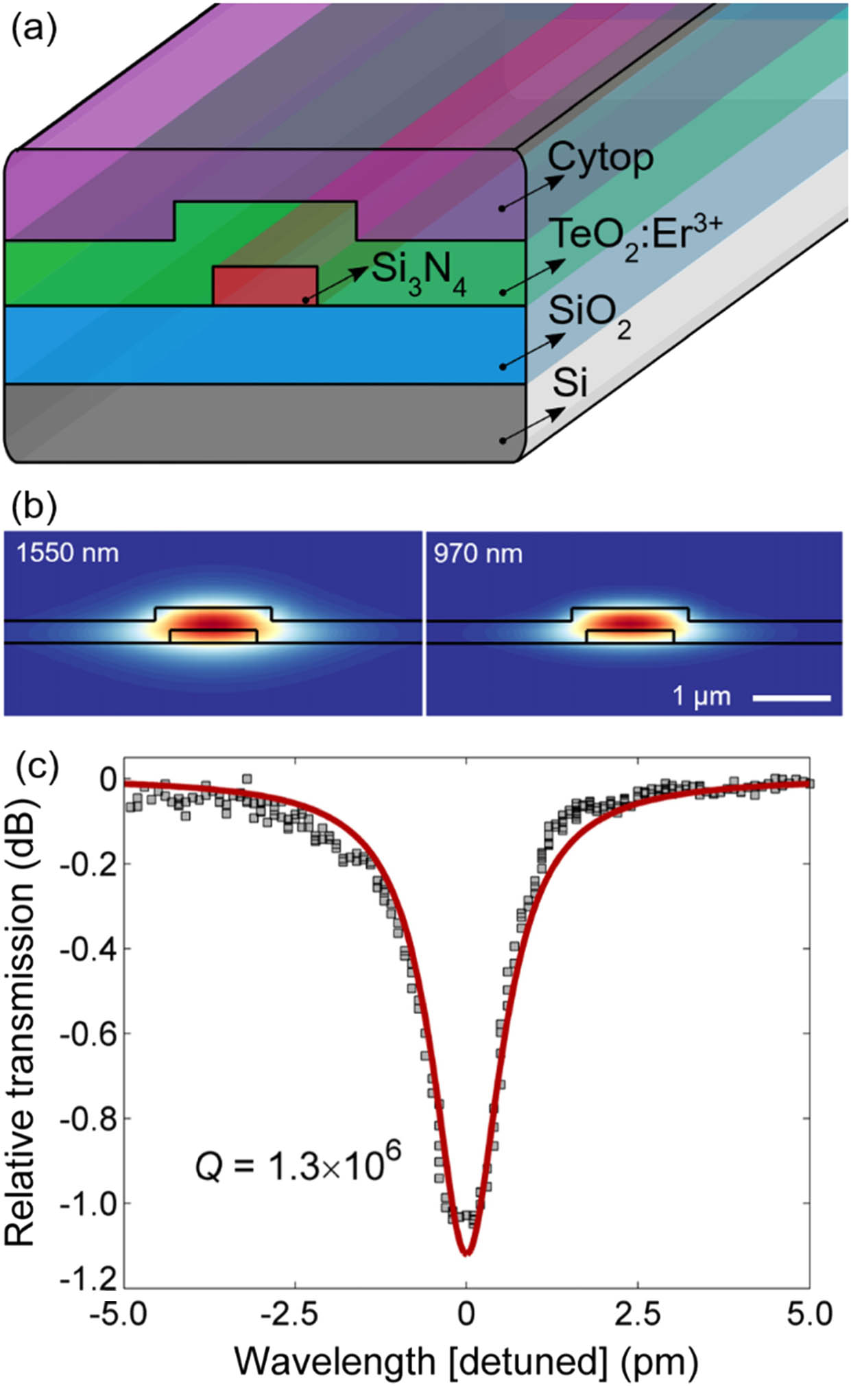
Figure 1.(a) Diagram of the -coated waveguide structure. (b) Calculated optical electric-field profile for the fundamental 1550 and 970 nm TE waveguide modes. (c) Resonance spectrum of a -coated waveguide ring resonator with a 400 μm radius and 2.6 μm nominal gap at a wavelength of 1637 nm. The data is fit using coupled mode theory to extract an intrinsic factor of corresponding to 0.25 dB/cm waveguide loss.
We estimated the erbium concentration in the coating using a prism coupling system by measuring the propagation loss of the film coated onto an unpatterned 6 μm thick thermal oxide sample at wavelengths from 1510 to 1640 nm. The loss at each wavelength was fit to its corresponding erbium absorption cross section, based on the values measured in Ref. [40], extracting an erbium concentration of and a background film propagation loss of .
The -coated silicon nitride ring resonator chip was used to characterize the background waveguide propagation loss. A 400 μm radius ring resonator with a 2.6 μm nominal ring-to-bus coupling gap was measured at wavelengths from 1630 to 1640 nm, which is assumed to have negligible erbium absorption and represent the passive waveguide loss of the structure. Figure 1(c) shows a resonance mode measured at 1637 nm, which we fit based on coupled mode theory to have an intrinsic factor of . This corresponds to a waveguide loss of approximately 0.25 dB/cm, which represents an improvement to the waveguide losses of 0.8 dB/cm [41] and 0.5 dB/cm [42] previously reported in this waveguide structure.
Two fiber-chip coupling setups, one active and one passive, are used to characterize the amplifier devices. We carry out gain measurements using a double-side pumping setup as shown in Fig. 2(a). The input side combines a tunable C-band (1530–1565 nm) signal laser with either a 970 or 1470 nm pump laser diode using a wavelength division multiplexer (WDM). We then edge-couple this light onto the chip, directly into the erbium-doped tellurium-oxide-coated silicon nitride waveguide structure from a 2.5 μm spot size tapered fiber. The waveguide supports a single TE polarized mode only [41], which the polarization paddles are optimized to launch into. We then couple light from the end facet of the waveguide into a similarly tapered fiber, after which the pump and signal light are separated by a second WDM. On the pump side arm is a second pump source laser diode, which travels backwards into the output side lensed fiber and onto the chip, allowing the waveguide to be pumped from both facets. The outcoupled signal light travels through a 1500 nm edge-pass filter to remove any residual pump remaining after the WDM, after which the transmitted signal is measured on a photodetector. Because the narrow bandwidth of the WDMs limits the wavelength range that can be detected to between 1530 and 1570 nm, we use a second passive characterization setup to be able to characterize samples at wavelengths from 1460 to 1640 nm. This setup removes the pump diodes, WDMs, and edge-pass filter, coupling the tunable laser directly onto and off the chip, with transmission measured on a photodetector. Using these setups, we used two different waveguides from the chip to characterize the amplification results of the platform, a 2.2 cm long straight waveguide and a 6.7 cm long paperclip waveguide in the shape shown in Fig. 2(b).

Figure 2.(a) Diagram of the double-side pumping setup used to measure gain on the -coated chips. (b) Image of the chip showing the characteristic green light emission of erbium when pumping the paperclip waveguide.
We initially tested the waveguides in the passive measurement setup to characterize facet and erbium absorption losses. A transmission spectrum for each waveguide from 1460 to 1640 nm was measured by sweeping the tunable laser output. Using the waveguide loss of 0.25 dB/cm measured by the ring resonator [Fig. 1(c)], insertion losses at 1640 nm of 12.1 and 20.8 dB give total fiber-chip coupling losses (including both the input and output) of 11.5 and 19.1 dB for the 2.2 cm long and 6.7 cm long waveguides, respectively. The facet loss is assumed to be the same for all wavelengths. The large variability in facet quality between samples is a result of the uneven edge created by the dicing process. As shown previously, the quality of the edge facets can be improved to 5 dB of loss per facet using focused-ion-beam polishing [36]. We assume that the 0.25 dB/cm of background waveguide loss and facet losses measured at 1640 are constant for all wavelengths measured. Therefore, any additional insertion loss measured at other wavelengths relative to the insertion loss measured at 1640 nm can be considered the result of erbium absorption loss. The measured absorption loss per unit length for both the 2.2 cm long and the 6.7 cm long waveguides around 1550 nm is shown in Fig. 3(a), with peak absorption of approximately 3.2 dB/cm occurring at a 1531 nm wavelength. Similarly, the erbium absorption around 970 nm was measured using a 970 nm tunable laser and the 2.2 cm long waveguide, shown in the inset of Fig. 3(a), with peak absorption of approximately 2.1 dB/cm at a 969 nm wavelength. We then measured the emission spectrum by optically pumping one of the end facets of the 2.2 cm long waveguide using the gain setup, with 50 mW of launched 970 nm pump power and measuring the back-collected amplified spontaneous emission (ASE) on an optical spectrum analyzer. The inset of Fig. 3(b) shows the measured erbium emission power versus wavelength, extending from 1460 to 1640 nm, with an emission peak at 1532 nm. We also used the back-collected ASE to characterize the waveguide’s excited-state lifetime by modulating the pump source at a 100 Hz frequency and measuring the decay of the ASE intensity versus time after the pump source has been turned off as shown in Fig. 3(b). We fit the luminescent decay with an exponential curve to yield an excited-state lifetime of 0.48 ms. In Refs. [39,43] it was shown that the excited-state lifetime is strongly related to the OH concentration present in the glass and that the excited-state lifetime of thin films can reach , even at large ion concentrations, by reducing OH concentration. High-purity sputtering targets, improved vacuum chamber base pressures, and heating samples to drive out OH incorporation in the film can potentially be used in the future to improve the excited-state lifetimes of the films.
Figure 3.(a) Erbium absorption loss from 1460 to 1640 nm measured in 2.2 and 6.7 cm long -coated waveguides. Inset: Erbium absorption loss from 940 to 980 nm in a 2.2 cm long -coated waveguide. (b) Measured back-collected photoluminescence intensity from the waveguide after the 1470 nm pump source has been turned off, fit to have an excited-state lifetime of 480 μs. Inset: Amplified spontaneous emission spectrum measured in a -coated waveguide.
We carried out small signal gain measurements using the gain setup depicted in Fig. 2(a). We swept the tunable signal laser from 1530 to 1570 nm and measured the transmitted power across the sample using the photodetector. To achieve internal net gain, the measured signal enhancement must overcome the waveguide erbium absorption loss, measured during absorption cross section calculation, and the background waveguide loss. We adjusted the tunable laser power such that the incident signal power at the input facet of the chips was , resulting in approximate launched signal powers of and for the 2.2 and 6.7 cm waveguide, respectively. No significant change in net gain was measured when the incident signal power was increased to the maximum available 0 dBm, corresponding to and of launched signal power. A incident signal power is used to maintain transmitted powers significantly above the ASE from the waveguide that also reaches the photodetector. To correct for ASE being detected as signal enhancement during gain measurements, we measured the ASE at each pump power with the signal laser turned off. We then subtracted that value from the measured transmission with the signal power on. The incident pump power was characterized by measuring the output power from the fiber with a free-space photodetector. The maximum combined incident pump powers were found to be 230 and 200 mW for the 970 and 1470 nm diodes, respectively. To find the total pump power launched into the waveguide and account for the fact that only the total facet loss—and not the loss at each facet—is known, during gain measurements the incident pump power from each side of the chip was set to be equal. The total launched pump power is then equal to the total incident power divided by the previously characterized total fiber-chip coupling loss. Pumping the waveguides from a single side and assuming the launched power is equal to the incident power divided by half the total fiber-chip coupling loss yields results that follow a similar gain versus launched pump power trend line to the data measured when pumping from both sides. This suggests similar total net gain would be achieved if sufficient pump power could be launched from a single facet.
Figure 4(a) shows the measured internal net gain versus launched pump power for the 2.2 cm long straight waveguide for both 970 and 1470 nm pump wavelengths. For this sample the total gain reaches 3.8 and 3.1 dB at a 1533 nm signal wavelength, which corresponds to gain per unit length of 1.7 and 1.4 dB/cm for 970 and 1470 nm pump wavelengths, respectively. As seen in Fig. 4(a), the gain begins to reach saturation after approximately 60 mW of launched pump power. The slightly higher gain measured for the 970 nm versus 1470 nm pump is the result of the resonant pumping effect, which particularly limits the ion population inversion and peak gain at 1533 nm, as can be seen in the flatter gain versus wavelength curve at maximum pump power for 1470 versus 970 nm pumping in Fig. 4(b). The net gain for both pump wavelengths converges to similar values at longer wavelengths where the resonant pumping effect is weaker.
Figure 4.Gain measurements in a 2.2 cm long -coated straight waveguide. (a) Internal net gain dependence on launched pump power for 970 and 1470 nm pump wavelengths and 1533 nm signal wavelength. (b) Internal net gain versus wavelength at maximum pump power for 970 and 1470 nm pump wavelengths.
The net gain versus launched pump power at 1558 nm signal wavelength for the 6.7 cm long waveguide is shown in Fig. 5(a). Because of the larger fiber-chip coupling loss associated with the longer waveguide, the pump power that can be launched onto the chip is limited to approximately 40 mW for both pump wavelengths. The internal net gain reaches 1.1 and 5.0 dB, corresponding to 0.2 and 0.8 dB/cm gain per unit length for 970 and 1470 nm pump wavelengths, respectively. For 1470 nm pumping, over 3 dB gain is achieved across the C band in this sample. The gain curves show that the launched pump power does not become high enough for the waveguide to reach gain saturation, which is the primary reason for the reduced gain per unit length seen in this sample. Additionally, the gain spectrum of Fig. 5(b), which displays the gain versus wavelength at peak pump power, shows peak gain occurring at 1558 nm instead of 1533 nm, another sign that gain saturation has yet to be reached.
Figure 5.Gain measurements in a 6.7 cm long -coated paperclip waveguide. (a) Measured (dashed lines/circles) and simulated (solid lines) internal net gain versus launched pump power for 970 and 1470 nm pump wavelengths and 1558 nm signal wavelength. (b) Internal net gain versus wavelength at maximum pump power for 970 and 1470 nm pump wavelengths.
The waveguide amplifier was modeled using a three-energy-level erbium rate equation model, including the effects of stimulated transitions, spontaneous decay, energy transfer upconversion, and ion quenching, similar to the model described in Refs. [19,44]. A diagram of the transitions used in the model can be seen in Fig. 6(a). The stimulated absorption and emission cross sections between the and levels are based on the results measured in ridge waveguides [40]. The stimulated transition cross section between the and levels is based on the 970 nm erbium absorption measured in this waveguide [Fig. 2(a)], divided by the simulated 70% confinement for 970 nm light in the layer and measured ion concentration, resulting in an estimated absorption cross section at the 969 nm wavelength peak. It is assumed that the emission cross section near the absorption peak will have the same value as the absorption cross section. Energy transfer upconversion parameters and excited-state lifetimes measured in tellurite fiber have been reported as and 3.3 and 0.26 ms for the and state, respectively [45]. However, as shown earlier, the lifetime of 0.48 ms measured in this waveguide structure is significantly lower than that reported in fiber, due to factors such as OH contamination. Therefore, the state lifetime used in the model is reduced by the same ratio to be 0.04 ms. A summary of the parameters used in the model can be found in Table 1.
Figure 6.(a) Three-level rate equation model diagram, showing processes of stimulated transitions (S), spontaneous decay (t), and energy transfer upconversion (W). (b) Measured net gain in 6.7 cm long waveguide, compared to simulated gain with 0%, 22.5%, and 40% quenched ions.
| Parameter | Value |
| Er3+ ion concentration | 2.2×10²⁰ ions/cm3 |
| 970 nm background propagation loss | 2.5 dB/cm |
| 1470 nm background propagation loss | 0.25 dB/cm |
| 1558 nm background propagation loss | 0.25 dB/cm |
| Launched signal power | −20 dBm |
| Upconversion parameter | 2.7×10⁻¹⁸ cm3/s |
| I13/24 lifetime | 0.48 ms |
| I11/24 lifetime | 0.04 ms |
| 970 nm absorption/emission cross section | 2.8/2.8×10−20 cm2 |
| 1470 nm absorption/emission cross section | 3.0/0.4×10−20 cm2 |
| 1558 nm absorption/emission cross section | 3.5/4.4×10−20 cm2 |
Table 1. Parameters Used for the Rate Equation Model
The model is used to fit the measured gain of the 6.7 cm long waveguide at a 1558 nm signal wavelength pumped with 1470 nm light. To accurately model the data, a fraction of the ions being fast quenched must be accounted for, where the quenched ions have excited-state lifetimes on the order of 1 μs for both the and excited states [19,44]. The fraction of quenched ions in the rate equation model is varied to most accurately fit the measured data, and it is found to be approximately 22.5% quenched ions as shown by the fit in Fig. 6(b). A 22.5% quenched ion fraction is comparable to the quenching fraction measured in waveguide amplifiers at similar ion concentrations of around [44]. The simulations demonstrate how significantly amplifier performance can be improved by reducing the fraction of quenched ions in the gain material. A waveguide amplifier with no quenched ions is predicted to have almost twice the measured gain reported in this sample. High-purity sputtering targets, heating films to anneal out defects as potential quenching sources, and co-doping of ytterbium atoms are all potential methods to reduce erbium ion quenching in the future.
Using the model, the total internal net gain in the 6.7 cm long waveguide sample is calculated [Fig. 5(a)] to reach 5.0 and 8.6 dB/cm at 150 mW of launched pump power for 970 and 1470 nm pump wavelengths, respectively, which could be achieved with improved fiber-chip coupling. Reaching gain saturation at reasonable launched pump powers () in the paperclip waveguide is more readily achievable using 1470 versus 970 nm pumping. The significantly reduced efficiency of the 970 nm pump in the longer waveguide sample can be attributed to the significantly larger background waveguide loss at 970 nm and potential loss around the bends from the waveguide becoming multimode near this wavelength. The 970 nm waveguide loss was found to be approximately 3.1 dB/cm based on previous results [38]. Using the same -coated ring resonator chip reported here, we measured the transmission around 940 nm in a 300 μm radius ring with a 1 μm bus waveguide-ring gap size and fit the resonance data to have a factor of (2.5 dB/cm loss). This factor confirms the larger background waveguide loss at this wavelength, which could be improved by reducing film loss and optimizing film thickness for 970 nm wavelength. The larger waveguide loss results in larger pump powers being required to invert the erbium ion population across the entire 6.7 cm long waveguide. In comparison, the low background waveguide loss around 1470 nm and high pump-signal overlap make it a highly efficient pump wavelength, requiring only 7 mW of launched pump power to reach the threshold for internal net gain.
The simulated net gain at a 1558 nm signal wavelength versus launched 1470 nm pump power for a waveguide amplifier with the same properties as the waveguides measured here for 5, 10, and 15 cm waveguide lengths is shown in Fig. 7(a). The results demonstrate that with no improvement to waveguide properties, high-quality waveguide amplifiers can be fabricated on this platform simply by optimizing waveguide length and fiber-chip coupling. A 10 cm long waveguide with 150 mW of pump power is simulated to have over 10 dB of net gain across the C band as shown in Fig. 7(b). Assuming a 300 μm minimum bend radius, a waveguide of this length could be patterned into a spiral amplifier with a sub- footprint area, representing a significant decrease in amplifier size compared to previously demonstrated spiral waveguide amplifiers, which are on the order of over [19,46].
Figure 7.Simulated net gain for -coated waveguides of 5, 10, and 15 cm length versus (a) launched 1470 nm pump power at a 1558 nm signal wavelength and (b) signal wavelength for 150 mW of launched 1470 nm pump power.
3. CONCLUSION
In summary, we have demonstrated erbium-doped waveguide amplifiers that are compatible with silicon nitride PIC technology. The -coated strip waveguides are fabricated using a standard foundry process and a single self-aligned deposition step. An internal net gain of 5 dB at 1558 nm has been achieved in a 6.7 cm-long waveguide. We have shown that such waveguide structures can have bend radii of without introducing any additional waveguide loss [41,42]. Simulations predict of gain across the C band in a compact amplifier by optimizing the fiber-chip coupling and waveguide length. These results demonstrate the possibility of fabricating ultra-compact -coated waveguide amplifiers that can reasonably achieve over 10 dB of total net gain. Further optimization of the excited-state lifetime and erbium doping concentration as well as reducing quenching can lead to even larger total net gain and EDWAs that can be fabricated on a tiny mass-producible silicon chip.
Acknowledgment
Acknowledgment. We acknowledge the Centre for Emerging Device Technologies (CEDT) at McMaster University and Shahram Tavakoli and Doris Stevanovic for support with fabrication.
References
[1] K. Wörhoff, R. G. Heideman, A. Leinse, M. Hoekman. TriPleX: a versatile dielectric photonic platform. Adv. Opt. Technol., 4, 189-207(2015).
[2] C. G. H. Roeloffzen, M. Hoekman, E. J. Klein, L. S. Wevers, R. Bernardus Timens, D. Marchenko, D. Geskus, R. Dekker, A. Alippi, R. Grootjans, A. van Rees, R. M. Oldenbeuving, J. P. Epping, R. G. Heideman, K. Wörhoff, A. Leinse, D. Geuzebroek, E. Schreuder, P. W. L. van Dijk, I. Visscher, C. Taddei, Y. Fan, C. Taballione, Y. Liu, D. Marpaung, L. Zhuang, M. Benelajla, K.-J. Boller. Low-loss Si3N4 TriPleX optical waveguides: technology and applications overview. IEEE J. Sel. Top. Quantum Electron., 24, 4400321(2018).
[3] J. F. Bauters, M. J. R. Heck, D. D. John, J. S. Barton, C. M. Bruinink, A. Leinse, R. G. Heideman, D. J. Blumenthal, J. E. Bowers. Planar waveguides with less than 0.1 dB/m propagation loss fabricated with wafer bonding. Opt. Express, 19, 24090-24101(2011).
[4] E. Shah Hosseini, S. Yegnanarayanan, A. Hossein Atabaki, M. Soltani, A. Adibi. High quality planar silicon nitride microdisk resonators for integrated photonics in the visible wavelength range. Opt. Express, 17, 14543-14551(2009).
[5] D. J. Blumenthal, R. Heideman, D. Geuzebroek, A. Leinse, C. Roeloffzen. Silicon nitride in silicon photonics. Proc. IEEE, 106, 2209-2231(2018).
[6] C. G. Roeloffzen, L. Zhuang, C. Taddei, A. Leinse, R. G. Heideman, P. W. van Dijk, R. M. Oldenbeuving, D. A. Marpaung, M. Burla, K. J. Boller. Silicon nitride microwave photonic circuits. Opt. Express, 21, 22937-22961(2013).
[7] R. M. De Ridder, K. Warhoff, A. Driessen, P. V. Lambeck, H. Albers. Silicon oxynitride planar waveguiding structures for application in optical communication. IEEE J. Sel. Top. Quantum Electron., 4, 930-937(1998).
[8] A. Fernández Gavela, D. Grajales García, J. Ramirez, L. Lechuga. Last advances in silicon-based optical biosensors. Sensors, 16, 285(2016).
[9] D. J. Moss, R. Morandotti, A. L. Gaeta, M. Lipson. New CMOS-compatible platforms based on silicon nitride and hydex for nonlinear optics. Nat. Photonics, 7, 597-607(2013).
[10] W. D. Sacher, J. C. Mikkelsen, Y. Huang, J. C. Mak, Z. Yong, X. Luo, Y. Li, P. Dumais, J. Jiang, D. Goodwill, E. Bernier, P. G. Q. Lo, J. K. S. Poon. Monolithically integrated multilayer silicon nitride-on-silicon waveguide platforms for 3-D photonic circuits and devices. Proc. IEEE, 106, 2232-2245(2018).
[11] E. Timurdogan, Z. Su, C. V. Poulton, M. J. Byrd, S. Xin, R. J. Shiue, B. R. Moss, E. S. Hosseini, M. R. Watts. AIM process design kit (AIMPDKv2. 0): silicon photonics passive and active component libraries on a 300 mm wafer. Optical Fiber Communications Conference and Exposition, 1-3(2018).
[12] Z. Fang, Q. Y. Chen, C. Z. Zhao. A review of recent progress in lasers on silicon. Opt. Laser Technol., 46, 103-110(2013).
[13] D. Nikolova, S. Rumley, D. Calhoun, Q. Li, R. Hendry, P. Samadi, K. Bergman. Scaling silicon photonic switch fabrics for data center interconnection networks. Opt. Express, 23, 1159-1175(2015).
[14] Y. Fan, J. P. Epping, R. M. Oldenbeuving, C. G. H. Roeloffzen, M. Hoekman, R. Dekker, R. G. Heideman, P. J. M. van der Slot, K.-J. Boller. Optically integrated InP-Si3N4 hybrid laser. IEEE Photon. J., 8, 1505111(2016).
[15] R. J. Mears, L. Reekie, I. M. Jauncey, D. N. Payne. Low-noise erbium-doped fibre amplifier operating at 1.54 μm. Electron. Lett., 23, 1026-1028(1987).
[16] C. G. Atkins, J. F. Massicott, J. R. Armitage, R. Wyatt, B. J. Ainslie, S. P. Craig-Ryan. High-gain broad spectral bandwidth erbium-doped fibre amplifier pumped near 1.5 μm. Electron. Lett., 25, 910-911(1989).
[17] Y. Sun, J. W. Sulhoff, A. K. Srivastava, J. L. Zyskind, T. A. Strasser, J. R. Pedrazzani, C. Wolf, J. Zhou, J. B. Judkins, R. P. Espindola, A. M. Vengsarkar. 80 nm ultra-wideband erbium-doped silica fibre amplifier. Electron. Lett., 33, 1965-1967(1997).
[18] J. D. B. Bradley, M. Pollnau. Erbium-doped integrated waveguide amplifiers and lasers. Laser Photon. Rev., 5, 368-403(2011).
[19] S. A. Vázquez-Córdova, M. Dijkstra, E. H. Bernhardi, F. Ay, K. Wörhoff, J. L. Herek, S. M. García-Blanco, M. Pollnau. Erbium-doped spiral amplifiers with 20 dB of net gain on silicon. Opt. Express, 22, 25993-26004(2014).
[20] J. Mu, M. Dijkstra, S. M. García-Blanco. Resonant coupling for active-passive monolithic integration of Al2O3 and Si3N4. IEEE Photon. Technol. Lett., 31, 771-774(2019).
[21] J. Mu, M. Dijkstra, Y. Yong, M. de Goede, L. Chang, S. M. García-Blanco. Monolithic integration of Al2O3 and Si3N4 toward double-layer active-passive platform. IEEE J. Sel. Top. Quantum Electron., 25, 8200911(2019).
[22] , J. Sun, T. N. Adam, G. Leake, D. Coolbaugh, J. D. B. Bradley, E. S. Hosseini, M. R. Watts. C- and L-band erbium-doped waveguide lasers with wafer-scale silicon nitride cavities. Opt. Lett., 38, 1760-1762(2013).
[23] M. Belt, T. Huffman, M. L. Davenport, W. Li, J. S. Barton, D. J. Blumenthal. Arrayed narrow linewidth erbium-doped waveguide-distributed feedback lasers on an ultra-low-loss silicon-nitride platform. Opt. Lett., 38, 4825-4828(2013).
[24] M. Belt, D. J. Blumenthal. Erbium-doped waveguide DBR and DFB laser arrays integrated within an ultra-low-loss Si3N4 platform. Opt. Express, 22, 10655-10660(2014).
[25] E. S. Hosseini, , J. D. B. Bradley, J. Sun, G. Leake, T. N. Adam, D. D. Coolbaugh, M. R. Watts. CMOS-compatible 75 mW erbium-doped distributed feedback laser. Opt. Lett., 39, 3106-3109(2014).
[26] , N. Li, E. S. Magden, G. Singh, N. Singh, A. Baldycheva, E. S. Hosseini, J. Sun, M. Moresco, T. N. Adam, G. Leake, D. Coolbaugh, J. D. B. Bradley, M. R. Watts. Ultra-narrow-linewidth Al2O3:Er3+ lasers with a wavelength-insensitive waveguide design on a wafer-scale silicon nitride platform. Opt. Express, 25, 13705-13713(2017).
[27] E. S. Magden, N. Li, , J. D. B. Bradley, N. Singh, A. Ruocco, G. S. Petrich, G. Leake, D. D. Coolbaugh, E. P. Ippen, M. R. Watts, L. A. Kolodziejski. Monolithically-integrated distributed feedback laser compatible with CMOS processing. Opt. Express, 25, 18058-18065(2017).
[28] N. Li, E. S. Magden, Z. Su, N. Singh, A. Ruocco, M. Xin, M. Byrd, P. T. Callahan, J. D. B. Bradley, C. Baiocco, D. Vermeulen, M. R. Watts. Broadband 2-μm emission on silicon chips: monolithically integrated holmium lasers. Opt. Express, 26, 2220-2230(2018).
[29] J. D. B. Bradley, E. S. Hosseini, , Z. Su, T. N. Adam, G. Leake, D. Coolbaugh, M. R. Watts. Monolithic erbium-and ytterbium-doped microring lasers on silicon chips. Opt. Express, 22, 12226-12237(2014).
[30] Z. Su, N. Li, E. S. Magden, M. Byrd, , T. N. Adam, G. Leake, D. Coolbaugh, J. D. B. Bradley, M. R. Watts. Ultra-compact and low-threshold thulium microcavity laser monolithically integrated on silicon. Opt. Lett., 41, 5708-5711(2016).
[31] N. Li, D. Vermeulen, Z. Su, E. S. Magden, M. Xin, N. Singh, A. Ruocco, J. Notaros, C. V. Poulton, E. Timurdogan, C. Baiocco, M. R. Watts. Monolithically integrated erbium-doped tunable laser on a CMOS-compatible silicon photonics platform. Opt. Express, 26, 16200-16211(2018).
[32] L. Wang, R. Guo, B. Wang, X. Wang, Z. Zhou. Hybrid Si3N4-Er/Yb silicate waveguides for amplifier application. IEEE Photon. Technol. Lett., 24, 900-902(2012).
[33] J. Rönn, W. Zhang, A. Autere, X. Leroux, L. Pakarinen, C. Alonso-Ramos, A. Säynätjoki, H. Lipsanen, L. Vivien, E. Cassan, Z. Sun. Ultra-high on-chip optical gain in erbium-based hybrid slot waveguides. Nat. Commun., 10, 432(2019).
[34] R. A. H. El-Mallawany. Tellurite Glasses Handbook: Physical Properties and Data(2012).
[35] V. A. G. Rivera, D. Manzani. Technological Advances in Tellurite Glasses: Properties, Processing, and Applications(2017).
[36] J. S. Wang, E. M. Vogel, E. Snitzer. Tellurite glass: a new candidate for fiber devices. Opt. Mater., 3, 187-203(1994).
[37] A. Jha, B. Richards, G. Jose, T. Teddy-Fernandez, P. Joshi, X. Jiang, J. Lousteau. Rare-earth ion doped TeO2 and GeO2 glasses as laser materials. Prog. Mater. Sci., 57, 1426-1491(2012).
[38] S. J. Madden, K. T. Vu. Very low loss reactively ion etched tellurium dioxide planar rib waveguides for linear and non-linear optics. Opt. Express, 17, 17645-17651(2009).
[39] K. Vu, S. Madden. Tellurium dioxide erbium doped planar rib waveguide amplifiers with net gain and 2.8 dB/cm internal gain. Opt. Express, 18, 19192-19200(2010).
[40] K. Vu, S. Farahani, S. Madden. 980 nm pumped erbium doped tellurium oxide planar rib waveguide laser and amplifier with gain in S, C and L band. Opt. Express, 23, 747-755(2015).
[41] H. C. Frankis, K. Miarabbas Kiani, D. B. Bonneville, C. Zhang, S. Norris, R. Mateman, A. Leinse, N. D. Bassim, A. P. Knights, J. D. B. Bradley. Low-loss TeO2-coated Si3N4 waveguides for application in photonic integrated circuits. Opt. Express, 27, 12529-12540(2019).
[42] H. C. Frankis, K. Miarabbas Kiani, D. Su, R. Mateman, A. Leinse, J. D. B. Bradley. High-Q tellurium-oxide-coated silicon nitride microring resonators. Opt. Lett., 44, 118-121(2019).
[43] S. Dai, C. Yu, G. Zhou, J. Zhang, G. Wang. Effect of OH-content on emission properties in Er3+-doped tellurite glasses. J. Non-Cryst. Solids, 354, 1357-1360(2008).
[44] L. Agazzi, K. Wörhoff, M. Pollnau. Energy-transfer-upconversion models, their applicability and breakdown in the presence of spectroscopically distinct ion classes: a case study in amorphous Al2O3:Er3+. J. Phys. Chem. C, 117, 6759-6776(2013).
[45] Y. Hu, S. Jiang, G. Sorbello, T. Luo, Y. Ding, B. Hwang, J. Kim, H. Seo, N. Peyghambarian. Numerical analyses of the population dynamics and determination of the upconversion coefficients in a new high erbium-doped tellurite glass. J. Opt. Soc. Am. B, 18, 1928-1934(2001).
[46] G. N. van den Hoven, R. J. I. M. Koper, A. Polman, C. van Dam, J. W. M. van Uffelen, M. K. Smit. Net optical gain at 1.53 μm in Er-doped Al2O3 waveguides on silicon. Appl. Phys. Lett., 68, 1886-1888(1996).


