• Journal of Semiconductors
  • Vol. 40, Issue 5, 052701 (2019)
Nasori Nasori1、2, Tianyi Dai3, Xiaohao Jia4、5, Agus Rubiyanto2, Dawei Cao3, Shengchun Qu4、5, Zhanguo Wang4、5, Zhijie Wang4、5, and Yong Lei1
Author Affiliations
  • 1Institute of Physics & IMN MacroNano ® (ZIK), Ilmenau University of Technology, 98693 Ilmenau, Germany
  • 2Physics Department, Faculty of Science, Institute of Technology Sepuluh Nopember, Surabaya, 6200, Indonesia
  • 3Department of Physics, Zhenjiang Key Laboratory for Advanced Sensing Materials and Devices, Faculty of Science, Jiangsu University, Zhenjiang 212013, China
  • 4Key Laboratory of Semiconductor Materials Science, Beijing Key Laboratory of Low Dimensional Semiconductor Materials and Devices, Institute of Semiconductors, Chinese Academy of Sciences, Beijing 100083, China
  • 5Center of Materials Science and Optoelectronics Engineering, University of Chinese Academy of Sciences, Beijing 100049, China
  • show less
    DOI: 10.1088/1674-4926/40/5/052701 Cite this Article
    Nasori Nasori, Tianyi Dai, Xiaohao Jia, Agus Rubiyanto, Dawei Cao, Shengchun Qu, Zhanguo Wang, Zhijie Wang, Yong Lei. Realizing super-long Cu2O nanowires arrays for high-efficient water splitting applications with a convenient approach[J]. Journal of Semiconductors, 2019, 40(5): 052701 Copy Citation Text show less
    (Color online) Schematic illustration of the whole fabrication procedure of Cu2O NWs by AAO template: gold layer deposition (I), Ni electrodeposition (II), aluminum and barrier layer removal (III), Cu2O growth (IV), and template removal (V).
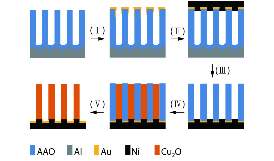
    Fig. 1. (Color online) Schematic illustration of the whole fabrication procedure of Cu2O NWs by AAO template: gold layer deposition (I), Ni electrodeposition (II), aluminum and barrier layer removal (III), Cu2O growth (IV), and template removal (V).
    (Color online) SEM images of (a) the as-prepared AAO template, (b) Cu2O NWs (inset is cross-sectional SEM image of Cu2O NWs) and (c) Cu2O films. (d) The corresponding XRD patterns of Cu2O NWs and films (inset is mapping of Cu2O NWs).
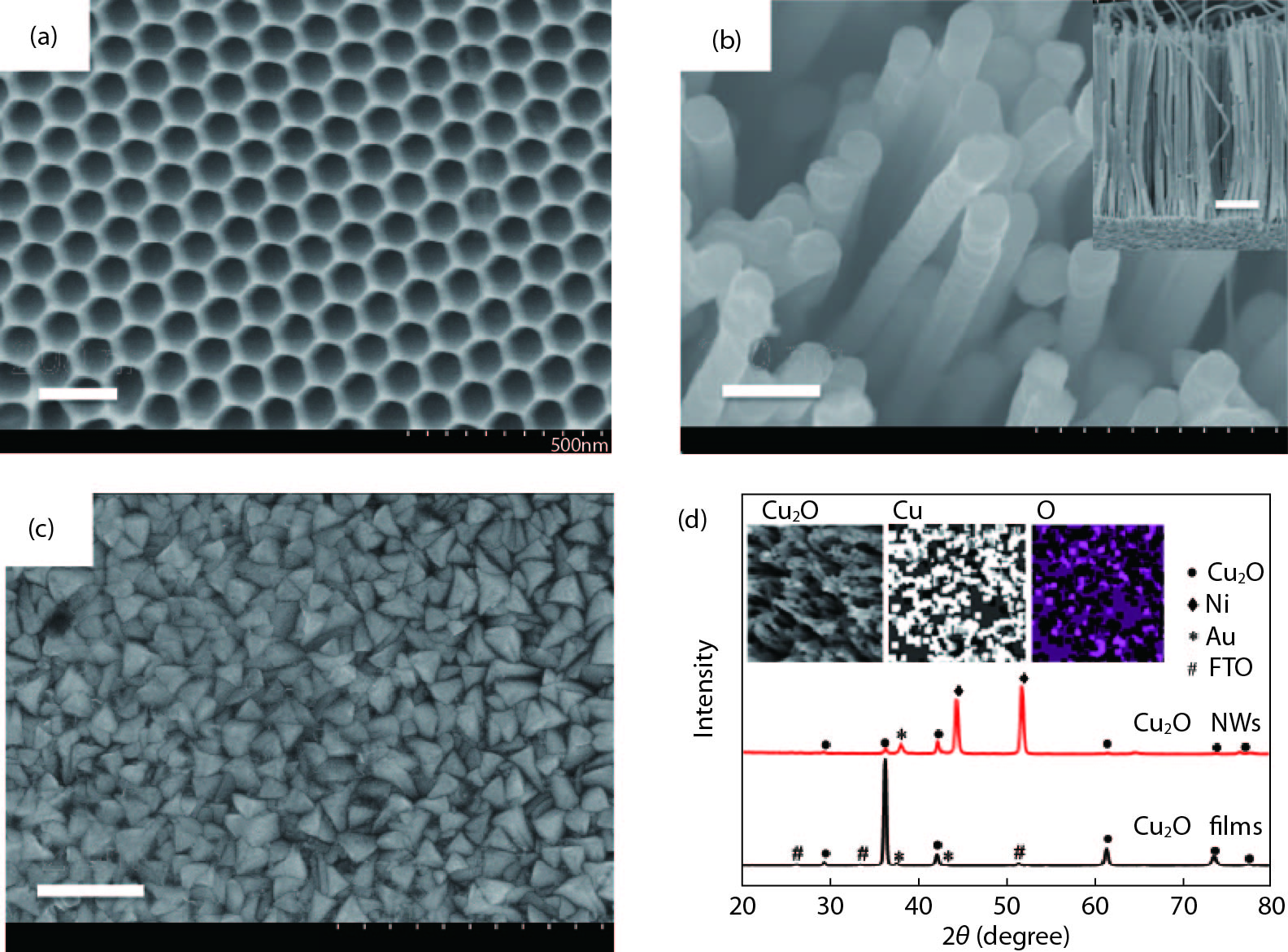
    Fig. 2. (Color online) SEM images of (a) the as-prepared AAO template, (b) Cu2O NWs (inset is cross-sectional SEM image of Cu2O NWs) and (c) Cu2O films. (d) The corresponding XRD patterns of Cu2O NWs and films (inset is mapping of Cu2O NWs).
    (Color online) (a) EQY spectra, (b) photocurrent–potential profiles, (c) time-dependent photocurrent density spectra and (d) impedance spectra of the Cu2O NWs and films photoelectrode.
    Fig. 3. (Color online) (a) EQY spectra, (b) photocurrent–potential profiles, (c) time-dependent photocurrent density spectra and (d) impedance spectra of the Cu2O NWs and films photoelectrode.
    (Color online) (a) Top-view SEM image of Cu2O NWs with Pt NPs. (b) Photocurrent–potential curves and (c) photocurrent-time profile at –0.3 V versus Ag/Ag and (d) EQY spectra of the photoelectrode based on Cu2O NWs with Pt NPs. The inset is impendence spectra.
    Fig. 4. (Color online) (a) Top-view SEM image of Cu2O NWs with Pt NPs. (b) Photocurrent–potential curves and (c) photocurrent-time profile at –0.3 V versus Ag/Ag and (d) EQY spectra of the photoelectrode based on Cu2O NWs with Pt NPs. The inset is impendence spectra.
    (Color online) (a) Schematic diagram of Cu2O NWs/Pt photoelectrode and (b) energy band-gap spectrum of the Cu2O NWs with/without Pt NPs.
    Fig. 5. (Color online) (a) Schematic diagram of Cu2O NWs/Pt photoelectrode and (b) energy band-gap spectrum of the Cu2O NWs with/without Pt NPs.
    Nasori Nasori, Tianyi Dai, Xiaohao Jia, Agus Rubiyanto, Dawei Cao, Shengchun Qu, Zhanguo Wang, Zhijie Wang, Yong Lei. Realizing super-long Cu2O nanowires arrays for high-efficient water splitting applications with a convenient approach[J]. Journal of Semiconductors, 2019, 40(5): 052701
    Download Citation