
Nasori Nasori, Tianyi Dai, Xiaohao Jia, Agus Rubiyanto, Dawei Cao, Shengchun Qu, Zhanguo Wang, Zhijie Wang, Yong Lei. Realizing super-long Cu2O nanowires arrays for high-efficient water splitting applications with a convenient approach[J]. Journal of Semiconductors, 2019, 40(5): 052701
- Journal of Semiconductors
- Vol. 40, Issue 5, 052701 (2019)
Abstract
1. Introduction
Since Fujishima and Honda initially, in 1972, reported hydrogen generation in a photoelectrochemical water splitting device by introducing the TiO2 electrode[
Cu2O, as an attractive candidate for light energy conversion, possessing a favorable direct band gap (Eg ~ 2.1 eV), which the maximum photocurrent in theory is of 15 mA/cm2 and the light-to-H2 conversion efficiency is 18% under a standard solar radiation[
2. Experimental
2.1. Preparation of Cu2O NWs and films
Synthesized from high purity Al foils, AAO templates were fabricated with a two-step anodization in oxalic acid (0.3 M) at 40 V during eight-hours anodization time for the first step and one-hour anodization time for the second step[
2.2. Fabrication of photocathodes of Cu2O NWs and films
The strip of conductive Cu tapes was connect to the uncovered FTO and Ni area of the FTO/Au/Cu2O and Ni/Cu2O NWs, respectively, in order to extend the conducting circuit. The Cu tapes were later put through the glass tubes, and then waterproofed with the a/b mixed epoxy adhesive. The area of samples was measured by a computer with the help of Photoshop software.
2.3. Measurements of PEC characteristics
The EQY measurement of the sample was obtained under a xenon lamp (150 W) with a grating monochromator from Newport corporation. Photocurrent–potential (J–V) curves and impedance characteristic were recorded by the high accuracy Bio-Logic potentiostat (SP-200) in sodium sulphate solution (0.1 M). A reference electrode (Ag/AgCl) and a counter electrode (Pt) were utilized during the measurements. As the light source, a standard 300 W xenon lamp (Newport) was used, and the optical intensity was set to 100 mW/cm2 with a standard Si solar cell from Newport corporation.
2.4. Characterizations of samples
The crystal structures and mapping of the Cu2O NWs and films were evaluated by measuring X-ray diffraction (XRD) spectra with Ni filtered Cu Kα radiation. The surface and cross-section morphologies of the samples were investigated using a scanning electron microscope (SEM, Hitachi S-570).
3. Results and discussion
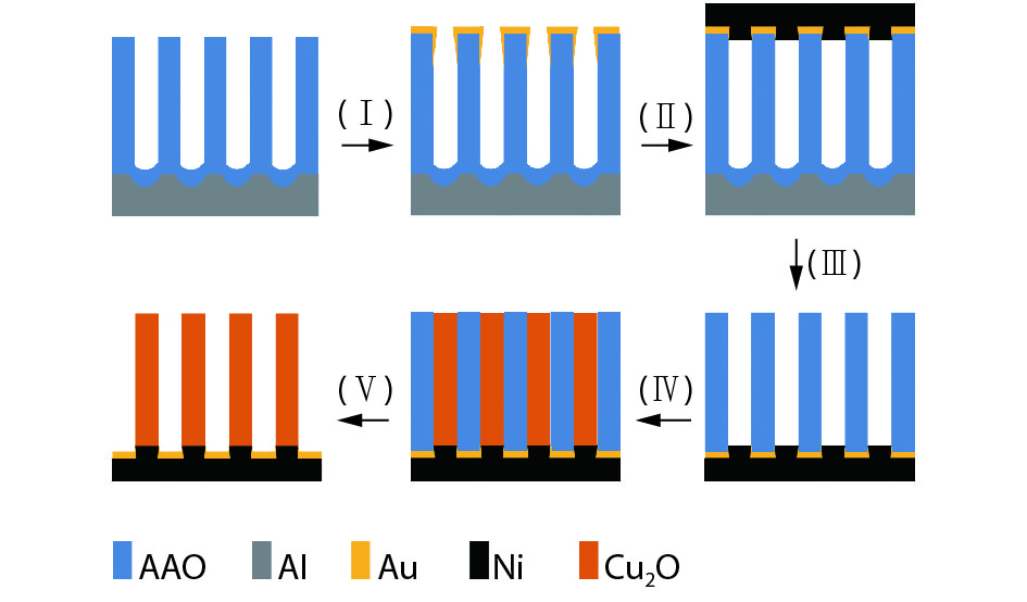
The whole fabrication procedure of Cu2O NWs can fall into 5 detailed processes that are presented schematically in Fig. 1, in which the colors of the Al, AAO, Au, Ni and Cu2O are illustrated as gray, blue, yellow, black and orange, respectively. The process includes gold layer deposition (I), Ni electrodeposition (II), aluminum and barrier layer removal (III), Cu2O growth (IV), and template removal (V). The AAO templates were employed as the main template during the preparation for the dramatic advantages, such as highly adjustable structural parameters, uniform and well oriented nano-porous structures, large surface area, cost-effective and good thermal stability and high mechanical strength[
![]()
Figure 1.(Color online) Schematic illustration of the whole fabrication procedure of Cu2O NWs by AAO template: gold layer deposition (I), Ni electrodeposition (II), aluminum and barrier layer removal (III), Cu2O growth (IV), and template removal (V).
Fig. 2(a) clearly illustrates that bare AAO template, which was fabricated with two times oxidization[
![]()
Figure 2.(Color online) SEM images of (a) the as-prepared AAO template, (b) Cu2O NWs (inset is cross-sectional SEM image of Cu2O NWs) and (c) Cu2O films. (d) The corresponding XRD patterns of Cu2O NWs and films (inset is mapping of Cu2O NWs).
In addition, the band gap of the grown films of Cu2O is measured as 2.1 eV by the UV–vis spectrums reported in our previous paper[
The corresponding XRD patterns of the Cu2O NWs and films are given in Fig. 2(d), where the diffraction peaks at 29.6°, 36.5°, 42.4°, 61.4° and 73.6° can be no doubtfully classified to the reflection of planes (110), (111), (200), (220) and (311) of the polycrystalline Cu2O, which are consistent with the No. 05-0667 in JCPDS card[
Fig. 3(a) demonstrates the typical stable state EQY curves of the photoelectrodes of Cu2O NWs and films. Comparing to Cu2O thin films photoelectrode, the Cu2O NWs photoelectrode on the nano-Ni exhibits an increscent EQY below the absorption threshold of Cu2O (600 nm). An enhancement of 2-fold is obtained, indicating that Cu2O NWs based electrode has a larger photo-to-current efficiency than that with Cu2O thin films. This result is consistent with those reported in recent studies that have focused on the outstanding light and electric properties of nanowires and improvement in photocatalytic performance of semiconductor nanowires[
![]()
Figure 3.(Color online) (a) EQY spectra, (b) photocurrent–potential profiles, (c) time-dependent photocurrent density spectra and (d) impedance spectra of the Cu2O NWs and films photoelectrode.
J–V curves were characterized by immersing the PEC electrodes in 0.1 M sodium sulfate solutions, with the reference of Ag/AgCl and the counter electrode of Pt wire. Each plot represents a typical photo-response obtained under simulative light source (AM 1.5 G, 100 mW/cm2), as illustrated in Fig. 3(b). These data reveal a cathodic photocurrent and imply a obvious p-type characteristic of both samples of Cu2O NWs and films, which are consistent with our previous report[
As illustrated in Fig. 3(c), to study the PEC performance and stability under visible light of samples, the time-dependent photocurrent (J–t) profiles of the Cu2O NWs and films was given with chopped light illumination (on: 250 s; off: 250 s) at –0.3 V versus Ag/AgCl. The results demonstrated that both samples exhibit photocurrent responses under each illumination quickly and reproducibly. The plateau photocurrent density of the Cu2O films electrode was –0.11 mA/cm2, while that of the Cu2O NWs was –0.71 mA/cm2, which represents a more 500% increase from the Cu2O films. The result demonstrates that nanostructure of materials can achieve the improvement of the photoelectric conversion, owing to the capability of offering large surface area and more reaction sites, decoupling light absorption and the collection of charge carrier, shorting diffusion distance of charge carrier compared to the bulk structures[
To elucidate the strong correlation between nanostructures and the enhanced photocurrent and EQY values, electrochemical impedance measurement was carried out. Fig. 3(d) shows Nyquist Impedance spectra of Cu2O NWs and films at DC frequency (200 kHz – 200 Hz) performed at open circuit voltage. In the electrolyte, Rct can be figured with fitting the semi-arc in 1 kHz region[
To further improve the performance of PEC in Cu2O nano-device, Pt NPs were deposited on the nanowire surrounds, which is the catalyst by a procedure of the ALD[
![]()
Figure 4.(Color online) (a) Top-view SEM image of Cu2O NWs with Pt NPs. (b) Photocurrent–potential curves and (c) photocurrent-time profile at –0.3 V versus Ag/Ag and (d) EQY spectra of the photoelectrode based on Cu2O NWs with Pt NPs. The inset is impendence spectra.
To shed light on the enhancement mechanism of PEC performance in Cu2O NWs with Pt NPs, the schematic illustration of Cu2O NWs/Pt photoelectrode and the total band energy spectrum of the Cu2O/Pt/electrolyte structure are schematically presented in Fig. 5. The bending band of Cu2O/Pt/electrolyte is similar to that case for p-Si/Pt/ electrolyte contact in a photoelectrochemical cell[
![]()
Figure 5.(Color online) (a) Schematic diagram of Cu2O NWs/Pt photoelectrode and (b) energy band-gap spectrum of the Cu2O NWs with/without Pt NPs.
4. Conclusion
In conclusion, we have shown that a novel photocathode based on super-long Cu2O NWs was successfully fabricated via the anodic alumina oxide template method. In comparison with the photocathode of Cu2O films, the Cu2O NWs photocathode demonstrates a significant enhancement in photocurrent, from –1.00 to –2.75 mA/cm2, attributing to advantages of the nanostructure including high specific surface area, light-trapping and short carriers transfer. After optimization of the photoelectrochemical electrode through depositing Pt NPs with ALD technology on the Cu2O NWs, the plateau of photocurrent has been enlarged to –7 mA/cm2 furthermore. This work provides a low-cost, naturally abundant nanowire material for application in photoelectrochemical cells.
Acknowledgements
This work was supported by European Research Council (HiNaPc: 737616), European Research Council (ThreeDsurface: 240144), BMBF (ZIK-3DNanoDevice: 03Z1MN11), DFG (LE 2249_4-1), BMBF (Meta-ZIK-BioLithoMorphie: 03Z1M511), National Natural Science Foundation of China (Nos. 21577086, 51702130, 21503209), Natural Science Foundation of Jiangsu Province (BK 20170550), Jiangsu Specially-Appointed Professor Program, Hundred-Talent Program (Chinese Academy of Sciences), Beijing Natural Science Foundation (No. 2162042) and Key Research Program of Frontier Science, CAS (No. QYZDB-SSW-SLH006).
References
[1] A Fujishima, K Honda. Electrochemical photolysis of water at a semiconductor electrode. Nature, 238, 37(1972).
[2] M Ni, M K H Leung, D Y C Leung et al. A review and recent developments in photocatalytic water-splitting using TiO2 for hydrogen production. Renew Sustain Energy Rev, 11, 401(2007).
[3] Z Zou, J Ye, K Sayama et al. Direct splitting of water under visible light irradiation with an oxide semiconductor photocatalyst. Nature, 414, 625(2001).
[4] S U M Khan, M Al-Shahry, W B Ingler. Efficient photochemical water splitting by a chemically modified n-TiO2. Science, 297, 2243(2002).
[5] M G Walter, E L Warren, J R McKone et al. Solar water splitting cells. Chem Rev, 110, 6446(2010).
[6] A J Bard, M A Fox. Artificial photosynthesis: solar splitting of water to hydrogen and oxygen. Acc Chem Res, 28, 141(1995).
[7] A Kudo, Y Miseki. Heterogeneous photocatalyst materials for water splitting. Chem Rev, 38, 253(2009).
[8] X Chen, S Shen, L Guo et al. Semiconductor-based photocatalytic hydrogen generation. Chem Rev, 110, 6503(2010).
[9] R Liu, Z Zheng, J Spurgeon et al. Enhanced photoelectrochemical water-splitting performance of semiconductors by surface passivation layers. Energy Environ Sci, 7, 2504(2014).
[10] S J A Moniz, S A Shevlin, D J Martin et al. Visible-light driven heterojunctionphotocatalysts for water splitting-a critical review. Energy Environ Sci, 8, 731(2015).
[11] D Cao, C Wang, F Zheng et al. High-efficiency ferroelectric-film solar cells with an n-type Cu2O cathode buffer layer. Nano Lett, 12, 2803(2012).
[12] M Hara, T Kondo, M Komoda et al. Cu2O as a photocatalyst for overall water splitting under visible light irradiation. Chem Commun, 3, 357(1998).
[13] C Xiang, G M Kimball, R L Grimm et al. 820 mV open-circuit voltages from Cu2O/CH3CN junctions. Energy Environ Sci, 4, 1311(2011).
[14] A Paracchino, V Laporte, K Sivula et al. Highly active oxide photocathode for photoelectrochemical water reduction. Nat Mater, 10, 456(2011).
[15] D Cao, N Nasori, Z Wang. Facile surface treatment on Cu2O photocathodes for enhancing the photoelectrochemical response. Appl Catal B, 198, 398(2016).
[16] G Ghadimkhani, N R de Tacconi, W Chanmanee et al. Efficient solar photoelectrosynthesis of methanol from carbon dioxide using hybrid CuO–Cu2O semiconductor nanorod arrays. Chem Commun, 49, 1297(2013).
[17] M Cao, C Hu, Y Wang et al. A controllable synthetic route to Cu, Cu2O, and CuO nanotubes and nanorods. Chem Commun, 1, 1884(2003).
[18] Y Tan, X Xue, Q Peng et al. Controllable fabrication and electrical performance of single crystalline cu2o nanowires with high aspect ratios. Nano Lett, 7, 3723(2007).
[19] J Zhang, J Liu, Q Peng et al. Nearly monodisperse Cu2O and CuO nanospheres: preparation and applications for sensitive gas sensors. Chem Mater, 18, 867(2006).
[20] Y Ben-Shahar, K Vinokurov, H de Paz-Simon et al. Photoelectrochemistry of colloidal Cu2O nanocrystal layers: the role of interfacial chemistry. J Mater Chem A, 5, 22255(2017).
[21] D P Singh, N R Neti, A S K Sinha et al. Growth of different nanostructures of Cu2O (nanothreads, nanowires, and nanocubes) by simple electrolysis based oxidation of copper. J Phys Chem C, 111, 1638(2007).
[22] Z Wang, D Cao, R Xu et al. Realizing ordered arrays of nanostructures: A versatile platform for converting and storing energy efficiently. Nano Energy, 19, 328(2016).
[23] Y Lei, L D Zhang, G W Meng et al. Preparation and photoluminescence of highly ordered TiO2 nanowire arrays. Appl Phys Lett, 78, 1125(2001).
[24] Y Lei, W Cai, G Wilde. Highly ordered nanostructures with tunable size, shape and properties: A new way to surface nano-patterning using ultra-thin alumina masks. Prog Mater Sci, 52, 465(2007).
[25] Y Lei, S Yang, M Wu et al. Surface patterning using templates: concept, properties and device applications. Chem Soc Rev, 40, 1247(2011).
[26] H Azimi, S Kuhri, A Osvet et al. Effective ligand passivation of Cu2O nanoparticles through solid-state treatment with mercaptopropionic acid. J Am Chem Soc, 136, 7233(2014).
[27] M Law, L E Greene, J C Johnson et al. Nanowire dye-sensitized solar cells. Nat Mater, 4, 455(2005).
[28] P J Pauzauskie, P Yang. Nanowire photonics. Mater Today, 9, 36(2006).
[29] H Sun, J Deng, L Qiu et al. Recent progress in solar cells based on one-dimensional nanomaterials. Energy Environ Sci, 8, 1139-1159(2015).
[30] Q Zhang, G Cao. Nanostructured photoelectrodes for dye-sensitized solar cells. Nano Today, 6, 91(2011).
[31] F G Zheng, P Zhang, X F Wang et al. Photovoltaic enhancement due to surface-plasmon assisted visible-light absorption at the inartificial surface of lead zirconate-titanate film. Nanoscale, 6, 2915(2014).
[32] A Ibhadon, P Fitzpatrick. Heterogeneous photocatalysis: recent advances and applications. Catalysts, 3, 189-218(2013).
[33] P V Kamat. Graphene-based nanoarchitectures anchoring semiconductor and metal nanoparticles on a two-dimensional carbon support. J Phys Chem Lett, 1, 520(2010).
[34] I Oh, J Kye, S Hwang. Enhanced photoelectrochemical hydrogen production from silicon nanowire array photocathode. Nano Lett, 12, 298(2012).
[35]


Set citation alerts for the article
Please enter your email address

© Copyright 2018-2021 | Chinese Laser Press. All Rights Reserved 沪ICP备15018463号-20