• Acta Physica Sinica
  • Vol. 69, Issue 6, 060201-1 (2020)
Wei-Qin Li1、2、*, Zhi-Sheng Huo1, and Hong-Bin Pu1
Author Affiliations
  • 1School of Automation & Information Engineering, Xi’an University of Technology, Xi’an 710048, China
  • 2Department of Electronic Science and Technology, Xi’an Jiaotong University, Xi’an 710049, China
  • show less
    DOI: 10.7498/aps.69.20191543 Cite this Article
    Wei-Qin Li, Zhi-Sheng Huo, Hong-Bin Pu. Transient characteristics of electron beam induced current in dielectric and semiconductor sample[J]. Acta Physica Sinica, 2020, 69(6): 060201-1 Copy Citation Text show less

    Abstract

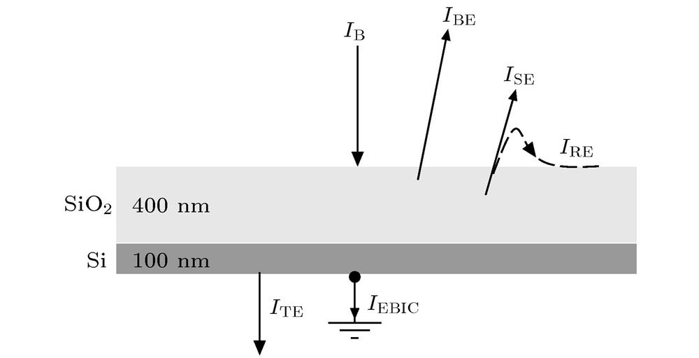
    The electron beam induced current (EBIC) characteristics of dielectric/semiconductor thin films under the electron beam (e-beam) irradiation is the important means of implementing the electron microscopic detection. The transient EBIC characteristics of the SiO2/Si thin film irradiated by a high-energy e-beam are investigated by combining the numerical simulation and the experimental measurement. The scattering process of electrons is simulated by the Rutherford scattering model and the fast secondary electron model, and the charge transport, trapping and the recombination process are calculated by the current continuity equation and the Poisson equation. The transient charge distribution, EBIC and the transmission current are obtained, and influence of the beam current and the beam energy on them are analyzed. The results show that due to the electron scattering effect, the free electron density decreases gradually along the incident direction. The net charge density near the surface is positive and negative along the incident direction because of secondary electrons (SEs) emitted from the surface, and therefore the electric field intensity is positive near the surface and negative inside sample, which causes some electrons to be transported to the substrate and some SEs return to the surface. The negative charge density at the SiO2/Si interface is higher than that in the nearby region because some electrons are trapped by the interface trap. With the decrease of the net charge density with e-beam irradiation, the charging intensity decreases gradually. Meanwhile, electrons are gradually transported to the substrate, and consequently EBIC and the sample current increase and the electric field intensity decreases with e-beam irradiation. However, due to the weak charging intensity, the surface emission current and the transmission current remain almost invariant with e-beam irradiation. The EBIC, the transmission current and the surface emission current are approximately proportional to the beam current. For the SiO2/Si thin film in this work, the transmission current increases gradually to the beam current value with the increase of the beam energy, and the EBIC presents a maximum value at the beam energy of about 15 keV.
    Wei-Qin Li, Zhi-Sheng Huo, Hong-Bin Pu. Transient characteristics of electron beam induced current in dielectric and semiconductor sample[J]. Acta Physica Sinica, 2020, 69(6): 060201-1
    Download Citation