
Lars Thylen, and Lech Wosinski. Integrated photonics in the 21st century[J]. Photonics Research, 2014, 2(2): 75
- Photonics Research
- Vol. 2, Issue 2, 75 (2014)
![Moore’s law for integration density in terms of equivalent number of elements per square micrometer of integrated photonics devices, showing a growth faster than the IC Moorés law, adapted from [3]. The figure covers, in time order, a lithium niobate 4×4 polarization-independent switch array, a 4×4 InP-based integrated gated amplifier switch array, an SOI AWG, and a hybrid plasmonic (passive) directional coupler. All these are experimentally demonstrated. At the top is a simulation of two coupled metal nanoparticle arrays, forming a directional coupler, each array being a resonantly operated array of silver nanoparticles. If loss requirements of, e.g., 3 dB/cm were invoked, the latter two would occupy significantly lower places in the figure.](/richHtml/prj/2014/2/2/02000075/img_001.jpg)
Fig. 1. Moore’s law for integration density in terms of equivalent number of elements per square micrometer of integrated photonics devices, showing a growth faster than the IC Moorés law, adapted from [3]. The figure covers, in time order, a lithium niobate 4 × 4 4 × 4 3 dB / cm
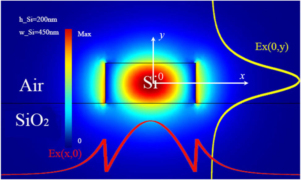
Fig. 2. Electric field distribution of TE mode in a silicon channel dielectric waveguide. The yellow and red curves express the amplitude distribution in the x and y directions, respectively; the substrate material is SiO 2 height = 200 nm width = 450 nm
Fig. 3. Ultrasmall subwavelength hybrid plasmonic microdisk. (a) Schematic diagram and (b) SEM image of the fabricated device with radius around 525 nm. At this radius the cavity has a resonance at about 1550 nm and the intrinsic quality factor Q SiO 2 0.08 dB / μm
Fig. 4. (a) Schematic diagram of the hybrid plasmonic microring modulator. (b) Cross-sectional view along the x–y plane of the Ez field distributions of a resonant mode at 1550 nm with an azimuthal number of 6. The modulator consists of an EOP ring with radius R and a width W sandwiched between a silver ring and a silicon ring with the same radii and widths. A microwave field is applied between the Ag cap and the bottom Si layer, and the refractive index of the EOP can be changed using the ultrafast EO (Pockels) effect; correspondingly, the cavity can be switched between on- and off-resonance modes at a given frequency, resulting in the modulation of transmission power if an access waveguide is placed aside.
|
Table 1. Waveguide Parameters for Different Materials
|
Table 2. Comparison of Performance of Some Electronically Controlled Modulatorsa ,b ,c

Set citation alerts for the article
Please enter your email address
© Copyright 2018-2021 | Chinese Laser Press. All Rights Reserved 沪ICP备15018463号-20