
Yang Shi, De Zhou, Yu Yu, Xinliang Zhang. 80 GHz germanium waveguide photodiode enabled by parasitic parameter engineering[J]. Photonics Research, 2021, 9(4): 605
- Photonics Research
- Vol. 9, Issue 4, 605 (2021)
Abstract
1. INTRODUCTION
Silicon photonics is promising for the demands of large-capacity data communications applications such as data centers, high-performance computers, and biomedical sensing [1,2]. One of the indispensable technologies in silicon photonics is high-speed signal detection for the near-infrared (), and germanium (Ge) is one of the most promising materials for near-infrared photodiodes (PDs) in optoelectronic integrated circuits due to its large absorption coefficient and compatibility with complementary metal-oxide-semiconductor (CMOS) technology [3]. Its superiority has led to substantial investigations of Ge PDs featuring high-frequency and responsivity in recent decades [4–10], while the parasitic parameters from either junction or electrodes limit a further increase in the bandwidth [11–13]. The Ge PDs can be divided into vertical and lateral positive-intrinsic-negative (PIN) junction structures. Although the bandwidth has achieved 120 GHz at for lateral ones [7], the dark current is very large and the fabrication processes are complex, requiring silicon corrosion and a Ge chemical mechanical polish [14,15]. On the other hand, vertical PIN PDs enjoy great popularity, for their simple fabrication processes. However, they suffer from low bandwidth due to high parasitic parameters [16,17]. Therefore, the parasitic parameters are optimized in different ways to overcome these issues, such as shrinking the intrinsic region to reduce the junction capacitance [11], optimizing silicon doping to reduce the series resistance [18], and introducing spiral inductors in the electrodes to offset part of capacitance effect [5]. However, all of these reported schemes optimize the parasitic parameters separately, without comprehensively considering the relationships between different aspects. For instance, in Ref. [11], only the junction capacitance is reduced, and the bandwidth is still limited by series resistance and electrode parasitic parameters. In addition, they also suffer from optical responsivity degradation or fabrication complexity.
In this work, we propose and demonstrate a high-speed Ge vertical PIN PD, by comprehensively optimizing the parasitic parameters from both junction and electrodes. An equivalent circuit model containing transit time and all parasitic parameters is considered. The bandwidth limit under a given intrinsic region size is investigated through two-dimensional (2D) joint optimization, by varying the silicon doping concentration and electrodes inductance. Experimentally, the bandwidth is enhanced from 27 to 80 GHz, with a low dark current of 6.4 nA and an optical responsivity of 0.89 A/W, leading to a high detectivity. This is, to the best of our knowledge, the highest bandwidth of a CMOS-compatible vertical Ge PIN PD reported to date. This work provides guidance for the design of high-speed and high-detectivity Ge PDs.
2. OPERATION PRINCIPLE
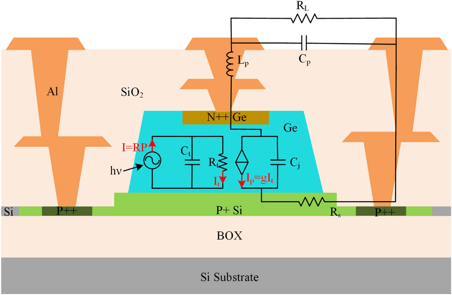
Figure 1.Cross-section view and equivalent circuit for a conventional PD.
The normalized frequency response of the radio frequency (RF) current through the load is shown in
Sign up for Photonics Research TOC. Get the latest issue of Photonics Research delivered right to you!Sign up now
![]()
Figure 2.(a) Simulated bandwidth varying with
As an implementation, the series resistance can be changed effectively by the silicon doping concentration calculated via the model in Ref. [22], as shown in Fig. 2(b). When the doping concentration increases, the resistance decreases until it reaches a constant of for the given footprint of silicon we adopted. The resistance of doped silicon will not be further reduced until , considering that the impurities cannot be completely ionized at a sufficiently high doping concentration [22]. The minimum of is mainly limited by the unchanged silicon-metal contact resistance of [18]. Based on the analyses above, the full doping is used in the whole silicon layer to minimize the resistance. On the other hand, for conventional ground-source-ground (GSG) electrodes, the is very small and can be significantly enlarged by introducing inductors of different lengths to generate a gain peaking effect [5,6]. When the inductance is about 240 pH, the bandwidth limit is for the minimum series resistance of 50 Ω, signed in Fig. 2(a). Note that other parasitic parameters remain almost unchanged for a fixed intrinsic region size, and it is reasonable to perform the 2D optimization for and . Thus, the theoretical limit can be obtained compared to the individual optimization.
3. FABRICATION AND EXPERIMENTAL RESULTS
![]()
Figure 3.(a) 3D schematic of the PD-A. (b) Cross-section of the PD-A with full silicon
The PDs are fabricated using an SOI wafer with an 220 nm thick silicon top layer and a 2 μm buried oxide (BOX). The grating coupler is first etched 70 nm from 220 nm silicon layer. After that, the silicon layer is etched into a ridge waveguide with a 90 nm slab for better light constraints. Then, the silicon top layer is or doping using different doses of boron. A 500 nm thick germanium is deposited on the doping region of the silicon, and depth doping of phosphorus is implanted on top of the Ge to form the vertical PIN junction. The area of the Ge is 5 μm wide and 10 μm in length. The first via and metal to Ge and silicon are fabricated; subsequently, the second via and metal are fabricated to form different inductors. PD-A, PD-B, and PD-REF were fabricated on the same wafer and at the same time.
A. Static Measurements
![]()
Figure 4.
B. Small-Signal Measurements
Small-signal RF measurements are carried out using a 67 GHz vector network analyzer (VNA: MS4647B, Anritsu Corp., Kanagawa, Japan) in the test range of 10 MHz to 70 GHz with 50 Ω load resistance. The impedance standard substrate [101-190C, FormFactor (formerly Cascade Microtech), Beaverton, OR, USA] is used to calibrate the bias-tee, cables, and microprobe (I67-GSG-150, FormFactor).
![]()
Figure 5.Measured and fitted bandwidth characteristics of Ge PDs.
4. DISCUSSION
To fairly characterize the proposed PDs, we take advantage of the concept of detectivity (), which is calculated using [24] Comparison of the High-Speed Waveguide-Coupled Ge PDsRefs. Type Dark Current (nA) Responsivity (A/W) Bandwidth (GHz) Detectivity ( [ Vertical 19 0.6 50 2.56 × 10⁹ [ Vertical 3000 0.75 60 6.85 × 10⁸ [ Vertical 61 0.85 67 4.30 × 10⁹ [ Lateral 4000 0.8 120 8.94 × 10⁸ [ Lateral 2.5 0.72 67 6.78 × 10⁹ [ Lateral 40 0.5 50 3.13 × 10⁹ This work Vertical 6.4 0.89 80 1.33 × 10¹⁰
5. CONCLUSION
We have demonstrated that 2D parasitic parameter engineering enables a significant bandwidth boost for Ge PDs. The bandwidth is experimentally enhanced from 27 to 80 GHz, and approaches the limit of 82 GHz. This method does not cause a degradation in responsivity and the dark current, which results in a very high detectivity. We believe it will pave the way toward the design of high-speed, high-detectivity Ge PDs.
References
[1] A. H. Atabaki, S. Moazeni, F. Pavanello, H. Gevorgyan, J. Notaros, L. Alloatti, M. T. Wade, C. Sun, S. A. Kruger, H. Y. Meng, K. Al Qubaisi, I. Wang, B. H. Zhang, A. Khilo, C. V. Baiocco, M. A. Popovic, V. M. Stojanovic, R. J. Ram. Integrating photonics with silicon nanoelectronics for the next generation of systems on a chip. Nature, 556, 349-354(2018).
[2] J. You, Y. K. Luo, J. Yang, J. H. Zhang, K. Yin, K. Wei, X. Zheng, T. Jiang. Hybrid/integrated silicon photonics based on 2D materials in optical communication nanosystems. Laser Photon. Rev., 14, 2000239(2020).
[3] J. Michel, J. F. Liu, L. C. Kimerling. High-performance Ge-on-Si photodetectors. Nat. Photonics, 4, 527-534(2010).
[4] H. T. Chen, P. Verheyen, P. De Heyn, G. Lepage, J. De Coster, P. Absil, G. Roelkens, J. Van Campenhout. High-responsivity low-voltage 28-Gb/s Ge p-i-n photodetector with silicon contacts. J. Lightwave Technol., 33, 820-824(2015).
[5] A. Novack, M. Gould, Y. S. Yang, Z. Xuan, M. Streshinsky, Y. Liu, G. Capellini, A. E. J. Lim, G. Q. Lo, T. Baehr-Jones, M. Hochberg. Germanium photodetector with 60 GHz bandwidth using inductive gain peaking. Opt. Express, 21, 28387-28393(2013).
[6] G. Y. Chen, Y. Yu, S. P. Deng, L. Liu, X. L. Zhang. Bandwidth improvement for germanium photodetector using wire bonding technology. Opt. Express, 23, 25700-25706(2015).
[7] L. Vivien, A. Polzer, D. Marris-Morini, J. Osmond, J. M. Hartmann, P. Crozat, E. Cassan, C. Kopp, H. Zimmermann, J. M. Fedeli. Zero-bias 40 Gbit/s germanium waveguide photodetector on silicon. Opt. Express, 20, 1096-1101(2012).
[8] H. Chen, P. Verheyen, P. De Heyn, G. Lepage, J. De Coster, S. Balakrishnan, P. Absil, W. Yao, L. Shen, G. Roelkens, J. Van Campenhout. −1 V bias 67 GHz bandwidth Si-contacted germanium waveguide p-i-n photodetector for optical links at 56 Gbps and beyond. Opt. Express, 24, 4622-4631(2016).
[9] L. Virot, D. Benedikovic, B. Szelag, C. Alonso-Ramos, B. Karakus, J. M. Hartmann, X. Le Roux, P. Crozat, E. Cassan, D. Marris-Morini, C. Baudot, F. Boeuf, J. M. Fedeli, C. Kopp, L. Vivien. Integrated waveguide PIN photodiodes exploiting lateral Si/Ge/Si heterojunction. Opt. Express, 25, 19487-19496(2017).
[10] J. F. Song, A. L. Eu-Jin, X. S. Luo, Y. Huang, X. G. Tu, L. X. Jia, Q. Fang, T. Y. Liow, M. B. Yu, G. Q. Lo. Microring resonator photodetector for enhancement in L-band performance. Opt. Express, 22, 26976-26984(2014).
[11] C. T. DeRose, D. C. Trotter, W. A. Zortman, A. L. Starbuck, M. Fisher, M. R. Watts, P. S. Davids. Ultra compact 45 GHz CMOS compatible germanium waveguide photodiode with low dark current. Opt. Express, 19, 24897-24904(2011).
[12] S. R. Liao, N. N. Feng, D. Z. Feng, P. Dong, R. Shafiiha, C. C. Kung, H. Liang, W. Qian, Y. Liu, J. Fong, J. E. Cunningham, Y. Luo, M. Asghari. 36 GHz submicron silicon waveguide germanium photodetector. Opt. Express, 19, 10967-10972(2011).
[13] L. Vivien, J. Osmond, J. M. Fedeli, D. Marris-Morini, P. Crozat, J. F. Damlencourt, E. Cassan, Y. Lecunff, S. Laval. 42 GHz p.i.n germanium photodetector integrated in a silicon-on-insulator waveguide. Opt. Express, 17, 6252-6257(2009).
[14] S. Lischke, D. Knoll, C. Mai, L. Zimmermann, A. Peczek, M. Kroh, A. Trusch, E. Krune, K. Voigt, A. Mai. High bandwidth, high responsivity waveguide-coupled germanium p-i-n photodiode. Opt. Express, 23, 27213-27220(2015).
[15] R. Going, T. J. Seok, J. Loo, K. Hsu, M. C. Wu. Germanium wrap-around photodetectors on silicon photonics. Opt. Express, 23, 11975-11984(2015).
[16] X. L. Li, Z. Liu, L. Z. Peng, X. Q. Liu, N. Wang, Y. Zhao, J. Zheng, Y. H. Zuo, C. L. Xue, B. W. Cheng. High-performance germanium waveguide photodetectors on silicon. Chin. Phys. Lett., 37, 038502(2020).
[17] T. Yin, R. Cohen, M. M. Morse, G. Sarid, Y. Chetrit, D. Rubin, M. J. Paniccia. 31 GHz Ge
[18] J. M. Lee, M. Y. Kim, W. Y. Choi. Series resistance influence on performance of waveguide-type germanium photodetectors on silicon. Chin. Opt. Lett., 15, 100401(2017).
[19] G. Wang, T. Tokumitsu, I. Hanawa, K. Sato, M. Kobayashi. Analysis of high speed pin photodiode S-parameters by a novel small-signal equivalent circuit model. IEEE Microw. Wireless Compon. Lett., 12, 378-380(2002).
[20] Y. Ishikawa, K. Wada. Near-infrared Ge photodiodes for Si photonics: operation frequency and an approach for the future. IEEE Photon. J., 2, 306-320(2010).
[21] M. Gould, T. Baehr-Jones, R. Ding, M. Hochberg. Bandwidth enhancement of waveguide-coupled photodetectors with inductive gain peaking. Opt. Express, 20, 7101-7111(2012).
[22] S. M. Sze, K. K. Ng. Physics of Semiconductor Devices(2006).
[23] J. Isenberg, W. Warta. Free carrier absorption in heavily doped silicon layers. Appl. Phys. Lett., 84, 2265-2267(2004).
[24] M. J. Deen, P. K. Basu. Silicon Photonics: Fundamentals and Devices(2012).

Set citation alerts for the article
Please enter your email address
© Copyright 2018-2021 | Chinese Laser Press. All Rights Reserved 沪ICP备15018463号-20