
Yushu Wang, Meng Li, Yu Wang, "Silk: a versatile biomaterial for advanced optics and photonics [Invited]," Chin. Opt. Lett. 18, 080004 (2020)
- Chinese Optics Letters
- Vol. 18, Issue 8, 080004 (2020)
![Schematic illustration of the development of advanced optical and multifunctional devices using silk building blocks based on its favorable material characteristics. Images reproduced with permission: “silk inverse opals”[15], copyright 2017, Wiley-VCH. “Optical fibers”[16], copyright 2009, Wiley-VCH. “DOEs”[17], copyright 2009, American Institute of Physics. “Bio-lasers”[18], copyright 2015, The Royal Society of Chemistry. “Plasmonic devices”[19], copyright 2015, American Chemical Society. “Metamaterials”[20], copyright 2020, Wiley-VCH. “Broadband reflection materials”[21], copyright 2018, Nature Publishing Group. “HOPs”[22], copyright 2019, Wiley-VCH. “Wrinkles”[23], copyright 2019, National Academy of Sciences.](/richHtml/col/2020/18/8/080004/img_001.jpg)
Fig. 1. Schematic illustration of the development of advanced optical and multifunctional devices using silk building blocks based on its favorable material characteristics. Images reproduced with permission: “silk inverse opals”[15], copyright 2017, Wiley-VCH. “Optical fibers”[16], copyright 2009, Wiley-VCH. “DOEs”[17], copyright 2009, American Institute of Physics. “Bio-lasers”[18], copyright 2015, The Royal Society of Chemistry. “Plasmonic devices”[19], copyright 2015, American Chemical Society. “Metamaterials”[20], copyright 2020, Wiley-VCH. “Broadband reflection materials”[21], copyright 2018, Nature Publishing Group. “HOPs”[22], copyright 2019, Wiley-VCH. “Wrinkles”[23], copyright 2019, National Academy of Sciences.
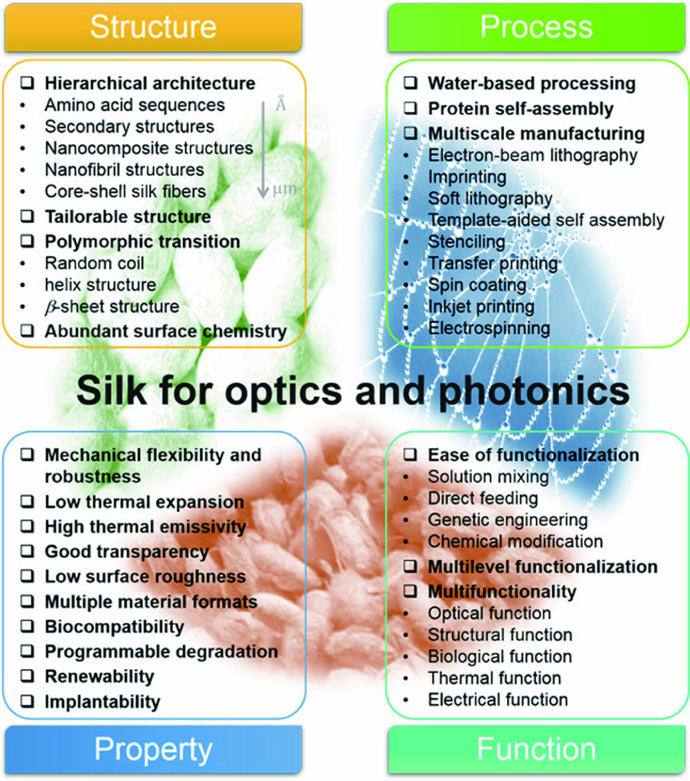
Fig. 2. Schematic representation of the inherent outstanding material characteristics of silk protein. The impressive balance of structure, process, property, and function makes silk distinct from other biopolymers.
Fig. 3. (a) Schematic of fabrication steps for large-scale patterned silk inverse opal. (b) Surface scanning electron microscopy (SEM) image and photograph (inset) of silk inverse opal templated from the colloidal multilayers composed of polystyrene spheres with a diameter of 300 nm. (c) Photograph of a bent silk inverse opal film showing viewing-angle-dependent structure color. (d) A floral pattern generated on silk inverse opal by selectively exposing part of the silk inverse opal to water vapor for different times. (e) A butterfly pattern on silk inverse opal by exposing masked silk inverse opal to UV light for different times. Reproduced with permission[15]. Copyright 2017, Wiley-VCH.
Fig. 4. (a) Schematic showing the generation of silk waveguides by (i) direct ink writing. Optical images of (ii) straight and (iii) wavy silk waveguides. Reproduced with permission[16]. Copyright 2009, Wiley-VCH. (b) Silk waveguide guiding light in tissue. Reproduced with permission[60]. Copyright 2015, Optical Society of America. (c) Surface SEM images of the silk fibers showing (i) debris and (ii) twisting on the fiber surface. (iii) Photographs of native silk fibers guiding light at 520 nm, 642 nm, and 730 nm. Reproduced with permission[61]. Copyright 2016, Nature Publishing Group. (d)(i) Surface SEM image of a native spider silk fiber. (ii) Micro-beam profile of a silk fiber during light injection. Reproduced with permission[32]. Copyright 2013, American Institute of Physics.
Fig. 5. (a) (i) AFM image (top) and diffraction pattern (middle) of a 2400 lines/mm silk grating. Bottom images in (i) are the enlarged AFM images of the 2400 and 3600 lines/mm silk gratings. (ii) Cycling of the hemoglobin-doped silk grating between the oxygenated (
Fig. 6. (a) Schematic and photograph of (i) the fabricated free-standing silk DFB laser and (ii) the emission spectra at different pump intensities. Reproduced with permission[18]. Copyright 2015, The Royal Society of Chemistry. (b) (i) Schematic of preparation of silk inverse structure and the corresponding SEM image of the final structure. (ii) The spectra of rhodamine 6G-doped silk above threshold and in fluorescence. Reproduced with permission[69]. Copyright 2016, Wiley-VCH. (c) (i) SEM images (top) and Fourier transforms amplitudes (bottom) of electrospun silk nanofibers assembled at different collection drum speeds, generating different degrees of nanofiber alignment. (ii) Lasing thresholds versus alignment degree AR (bottom x axis) and Young’s moduli of electrospun silk fibroin nanofibrous scaffolds (top x axis). Reproduced with permission[70]. Copyright 2017, Nature Publishing Group.
Fig. 7. (a) (i) Schematic of fabrication process of the plasmonic nanostructures with (1–4) nanodot structures and (5–8) nanohole structures using transfer fabrication technique. SEM images of transfer imprinted plasmonic nanodot arrays (1 and 2) and nanohole arrays (3 and 4) on rhodamine-B-doped silk films. Reproduced with permission[76]. Copyright 2012, Wiley-VCH. (b) (i) Schematic showing the fabrication process of the silk plasmonic absorber sensor. (ii) SEM (left) and AFM (right) images showing the morphology of Au on silk film. Reproduced with permission[19]. Copyright 2015, American Chemical Society.
Fig. 8. (a) (i) Schematic of the preparation of terahertz (THz) metamaterials on silk substrates using the shadow mask patterning technique. (ii) Microscopic image of the sprayed metamaterial arrays. (iii) Spectrum response of 60% humidity treated silk metamaterial composite with drying time. Reproduced with permission[79]. Copyright 2010, Wiley-VCH. (b) (i) Working principle of the degradable silk-based THz metamaterials. (ii) Camera and microscopic images of a portion of the THz metamaterials on silk film. (iii) Microscopic images (top) and transmission spectra (bottom) after immersing in deionized (DI) water for different times. Reproduced with permission[20]. Copyright 2020, Wiley-VCH.
Fig. 9. (a) Dark-field optical microscopy image of Argema mittrei cocoon silks (left) and cross-sectional SEM image showing the existence of voids with sizes ranging from hundreds of nanometers to one micron (right). (b) Reflectance and emissivity spectra of a single cocoon fiber from the visible to the mid-infrared. (c) Transverse (left) and longitudinal (right) cross-sectional SEM images of a regenerated silk fiber containing a high density of voids. Reproduced with permission[21]. Copyright 2018, Nature Publishing Group.
Fig. 10. (a) Schematic of fabrication process of silk-based hierarchical opals. (b) Surface SEM image of hierarchical opal with inset showing the cross-sectional SEM image. (c) Transmitted image of the “Tufts” words through diffuser-based hierarchical opal (left) and corresponding projected diffraction patterns in both reflection and transmission modes (right). (d) Photograph showing vivid structural color. (e) (Left) Diffraction patterns of pattern-generator-based hierarchical opals with different layers of inverse colloidal crystals. (Right) The variation of relative diffraction intensity, absolute reflection, and transmission intensity with the increase of layer numbers of inverse colloidal crystal. (f) Photograph of patterned hierarchical opal observed at the angles of 0° and 45°. Reproduced with permission[22]. Copyright 2019, Wiley-VCH.
Fig. 11. (a) Schematic illustration of the formation of silk wrinkling system. (b) Schematics (top) and photographs (bottom) of electricity-responsive dynamic wrinkling system, showing the reversible transition between transparent and opaque. (c) Schematics (top) and corresponding photographs (bottom) of patterned wrinkling surfaces generated by water-vapor exposure through using a shadow mask (left), by water ink-based inkjet printing (middle), and by fingerprinting (right). (d) Schematics of temperature measurement when a white-light beam passes through the wrinkle-free (left) or wrinkled (right) sample. Insets show the projected diffraction patterns. (e) The evolution of temperature during white-light on and off. Reproduced with permission[23]. Copyright 2019, National Academy of Sciences.


Set citation alerts for the article
Please enter your email address

© Copyright 2018-2021 | Chinese Laser Press. All Rights Reserved 沪ICP备15018463号-20