Abstract
The growing demand of sustainable and biocompatible optical devices is stimulating the development of naturally derived biomaterials for optics and photonics. As a versatile biomaterial, silk provides excellent material characteristics that are favorable towards the generation of advanced optical systems. This review examines the use of silk as a material platform in optical applications. Recent advances in silk-based optical devices and multifunctional devices are summarized. The challenges and directions in further designing and fabricating silk optics are also discussed. We envision that silk will play a pivotal role in the future exploitation of sustainable, intelligent, wearable/implantable, and multifunctional optical devices.1. INTRODUCTION
Optics and photonics are indispensable to the creation of new technologies that help to find solutions to various critical global challenges. The growing developments of optical technologies in energy, environmental, information, and biomedical applications are creating a demand for optical materials and devices that are not only sustainable but also implantable and bioresorbable[1–3]. However, it remains challenging to develop such optical materials and devices while maintaining prominent structural and optical performance. Naturally derived biomaterials, such as silk, cellulose, chitin, melanin, and DNA, provide a unique opportunity by being simultaneously “technological” (e.g., optically active, micro- and nanoscale processable), “structural” (e.g., rich surface chemistry, mechanical flexibility), “sustainable” (e.g., renewable, eco-friendly), and “biological” (e.g., biocompatible, biodegradable). These traits make them ideally suitable for applications at the interface between optical technologies and environment within humans or around humans[4,5].
Silks belong to a large family of structural proteins and are mainly synthesized by several arthropods, including silkworms and spiders[6–8]. Among the different sources, domestic Bombyx mori (B. mori) silks come from abundant sources and have been the main focus for multi-field applications. B. mori silks are well-known for their wide use in textiles and sutures because of their shimmering appearance, along with their soft texture, lightweight, and mechanical robustness. With the in-depth understanding of the material characteristics and the advancements in manufacturing technologies, the applications of such ancient biomaterials are transferred from traditional textile fields to advanced technical fields, including optics and photonics, energy, electronics, and optoelectronics[9–12].
Over the past decades, a tremendous increase in the use of silk protein for applications in optics and photonics has been witnessed due to its excellent balance of the “structure-process-property-function” relationship[9,13,14]. This review attempts to provide an overview of recent progress in advanced optical devices constructed from silk protein with a particular emphasis on the structural designs responsible for the final optical functionalities (Fig. 1). The goal of this study is to highlight the opportunities provided by silk towards the replacement of existing non-renewable optical platforms with environmentally friendly, biocompatible systems that match the high performance of the contemporary devices, while avoiding energy-intensive input, toxic byproducts, waste, and environmental degradation (Fig. 1). This review first outlines the justifications of using silk for optical applications, followed by a summary of the state-of-the-art silk-based optical devices. Next, a special focus is paid to the recent advances in silk-based multifunctional optical devices. Finally, we discuss the challenges and directions for further devising silk-based biomaterials for future sustainable, intelligent and adaptive, wearable/implantable, and multifunctional optical devices.
Sign up for Chinese Optics Letters TOC. Get the latest issue of Chinese Optics Letters delivered right to you!Sign up now
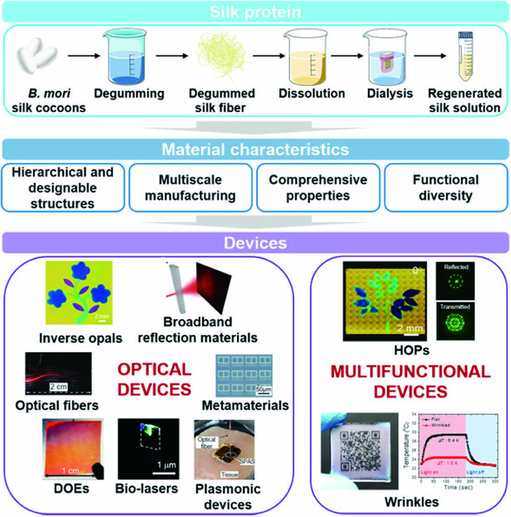
![Schematic illustration of the development of advanced optical and multifunctional devices using silk building blocks based on its favorable material characteristics. Images reproduced with permission: “silk inverse opals”[15], copyright 2017, Wiley-VCH. “Optical fibers”[16], copyright 2009, Wiley-VCH. “DOEs”[17], copyright 2009, American Institute of Physics. “Bio-lasers”[18], copyright 2015, The Royal Society of Chemistry. “Plasmonic devices”[19], copyright 2015, American Chemical Society. “Metamaterials”[20], copyright 2020, Wiley-VCH. “Broadband reflection materials”[21], copyright 2018, Nature Publishing Group. “HOPs”[22], copyright 2019, Wiley-VCH. “Wrinkles”[23], copyright 2019, National Academy of Sciences.](/Images/icon/loading.gif)
Figure 1.Schematic illustration of the development of advanced optical and multifunctional devices using silk building blocks based on its favorable material characteristics. Images reproduced with permission: “silk inverse opals”[15], copyright 2017, Wiley-VCH. “Optical fibers”[16], copyright 2009, Wiley-VCH. “DOEs”[17], copyright 2009, American Institute of Physics. “Bio-lasers”[18], copyright 2015, The Royal Society of Chemistry. “Plasmonic devices”[19], copyright 2015, American Chemical Society. “Metamaterials”[20], copyright 2020, Wiley-VCH. “Broadband reflection materials”[21], copyright 2018, Nature Publishing Group. “HOPs”[22], copyright 2019, Wiley-VCH. “Wrinkles”[23], copyright 2019, National Academy of Sciences.
2. OPPORTUNITY OF SILK AS A PLATFORM FOR OPTICS AND PHOTONICS
Among the promising candidates of biopolymers, silk proteins are particularly attractive to develop optical devices because of their unique material characteristics, which on top of their intrinsic favorable optical properties (transparency and average refractive index of 1.55 at ), include hierarchical and tailorable structures, multilevel processability, excellent mechanical, thermal, and biological properties, and ease of functionalization[13,14].
Native silks are produced from a liquid-crystal gel stored in animal glands via a “spinning” process, which differentiates them from other natural fibers such as hair and wool that are grown from tissue cells at a much slower rate[6]. As an exquisitely “invented” product of nature, silk fiber presents hierarchical architecture over multiple length scales, regardless of sources[24]. At the molecular level, silk is composed of a highly repetitive core and two structurally non-repetitive terminals (C and N)[25]. Within the repetitive core sequences, poly (Bombyx mori silks) or poly (spider silks) domains are hydrogen-bonded to form anti-parallel -sheet nanocrystals at the several nanometer length scale[26]. These nanocrystals are interspersed within less orderly amorphous domains to form protein nanocomposites, which are further organized into fibrils at tens to hundreds of nanometer scale[27]. Numerous tiny fibrils bundle together to form macroscopic silk fibers at micrometer dimensions. At the fiber scale, silk fibers can be considered to be core–shell protein fibers with a silk fibroin core (the major component) and a skin/shell layer (e.g., a skin layer of spider silk consisting of lipid, glycol, and protein[6,28] and a sericin shell for silkworm silks[7]). These hierarchical structures over multiple scales interact synergistically to endow silk with its enviable mechanical toughness through an unexceptionable balance of modulus, strength, and extensibility[29–31]. More interestingly, this hierarchical structural organization also contributes its exceptional optical properties (see details in the following section)[32–34].
The beauty of silk for developing optical devices is that not only can the silk fibers in their native formats be applied directly as the functional carriers, but also the regenerated silk proteins can be used as the building blocks to direct their assembly. Recent progress has been made in the progressing of silk materials. This relies on a regeneration process to transform the solid silk fibers into aqueous silk protein solutions. Taking B. mori silk for example, such a regeneration procedure is operated in an all-water-based environment, including (i) a degumming step to remove the sericin coating, (ii) rehydration of silk proteins through dissociating the hydrogen bonds between protein chains with the aid of chaotropic salts, and (iii) a dialysis step to obtain an aqueous solution of pure regenerated silk fibroin[35]. Starting from such a silk solution, diverse material formats including films, fibers, hydrogels, aerogels, sponges, and blocks can be generated by modulating the self-assembly of silk protein[36]. Such reconstructed silk materials show tailorable mechanical properties with a modulus ranging from hundreds of pascal (Pa) to several giga-pascal (GPa), promising the efficient match with different application environments. Benefiting from the water-based process at ambient temperature and pressure, this protein self-assembly process can be easily adapted to various multiscale manufacturing techniques (from nanoscale to macroscale) to create a wide range of forms for optical uses and, consequently, a broad variety of functions[14,36].
As a structural protein, silk fibroin is capable of controllable conformational transitions upon exposure, to such as water vapor, methanol, and UV light[37,38]. This capability provides a unique opportunity to modulate the material on the nanoscale, offering the possibility to create reconfigurable optics[15,39]. At the same time, as a biocompatible and biodegradable material, silk fibroin does not cause an inflammatory response, making it suitable for implantable optical devices that can be left in the body and are gradually resorbed by biological systems[40]. The dissolution and/or biodegradation rates can be tailored from minutes to years through controlling the abovementioned polymorphic transitions, enabling the emergence of physical transient optics that can be dissolved in a programmable way[41,42]. In addition, silk protein is also able to reversibly volume variation in response to external stimuli, including humidity, aqueous solvent, mechanical strain, and temperature, allowing the generation of dynamic tunable optics[43–46].
Furthermore, the ambient environment during silk processing enables the facile functionalization of silk materials through simple incorporation of biotic/abiotic components into the aqueous solution without loss of their bioactivity/function[47]. In addition to solution mixing, functions can also be enriched through either directly feeding silk worms with special diets[48], genetic engineering to insert specific domains into the molecular sequences of silk protein[49], or chemical modification of the protein by taking advantage of its abundant surface chemistry[50]. These capacities add new predesigned functions into silk materials, providing opportunities for developing multifunctional, environmentally interactive optical devices that are otherwise difficult to reach[17,41]. The confluence of all these distinctive material characteristics makes silk an optimal platform for a wide variety of optical devices and is summarized in Fig. 2.
Figure 2.Schematic representation of the inherent outstanding material characteristics of silk protein. The impressive balance of structure, process, property, and function makes silk distinct from other biopolymers.
All in all, silk fibroin has been proposed to be an ideal candidate for sustainable, biocompatible, wearable, implantable, and biofunctional optics. This opens up application opportunities where silk is used as a material to bridge optics and the biological world. In addition, the variable nature of silk protein in response to environmental fluctuations enables the development of reconfigurable, tunable, transient, and multifunctional optics, which together with the versatility of silk protein, is highly desirable for applications including biosensing and environmental sensing, smart textiles, disposable and bioabsorbable devices, drug delivery systems with self-monitoring capabilities, thermal management, and information coding.
3. SILK-PROTEIN-BASED OPTICAL DEVICES
A. Structural Color Materials
Structural colors have distinctive optical features such as iridescence, tunability, and resistance to fading, in comparison with pigmentary colors. Structural colors arise from the interaction of periodic nanostructures with light, such as through light diffraction, interference, scattering, or absorption. The seamless match between silk protein and the state-of-the-art nanomanufacturing technologies allows the creation of one-dimensional (1D), two-dimensional (2D), and three-dimensional (3D) photonic nanostructures to import structural color functions for silk materials.
1D photonic structures with thin film interference[51] or multilayer interference[52] can be easily obtained by depositing thin layers of silk by spin-coating, dip-coating, and spray-coating the aqueous solution. Silk-protein-based multilayer structures with humidity-stimulated fast structural color variations were fabricated[52]. This was achieved through an alternate layer-by-layer deposition of silk and silk/titanate composite film through a facile spin-coating approach. The introduction of titanate nanosheets into the silk matrix significantly increases its refractive index (from 1.56 to 1.82), enabling a Bragg diffraction peak centered at around 400 nm when ∼80 nm thick silk layer and ∼40 nm thick silk/titanate layer are used. Due to the high hydrophilicity of silk protein, this multilayer film exhibits fast and reversible humidity responsiveness and evident color variation in 5 s, showing the potential in applications for moisture sensors and anti-counterfeit labeling.
Silk-protein-based 2D photonic structures can be attained by combining protein self-assembly with nanoimprinting[53,54] or electron-beam lithography[55,56]. The capacity to tune the glass transition temperature of amorphous silk by adjusting its water content makes it possible to design nanopatterns by contact imprinting (that is, by bringing the silk film into contact with a nanopatterned mold) at different temperatures. Using this approach, 2D square lattices of air holes were generated[53]. Vivid structural colors with different hues can be obtained through controlling the lattice pitch. The master material is not limited to rigid silicon; instead, a dry crystallized silk fibroin film can also be used as a master[54]. This so-called “protein–protein imprinting” strategy enables the obtainment of multigeneration optical products with high quality. Energy inputs, such as electron irradiation, can induce the conformational changes of silk protein between the random coil, helix, and -sheet structure and, thus, the transition between water-soluble and -insoluble states. This feature allows the use of silk as either a positive or a negative resist in electron-beam lithography[55]. 2D photonic crystal patterns with nanohole arrays were created after the “water development” process when water-insoluble crystalline silk was locally exposed to an electron beam to induce the degradation of the silk molecular chains into water-soluble polypeptides. Conversely, nanopillar arrays were generated when water-soluble amorphous silk was exposed to a high-power electron beam to induce the conformational transition from amorphous to helix and, thus, to render silk protein in the exposed regions water-insoluble. In addition to controlling the lattice pitch, different diffractive colors can also be achieved by tuning the refractive index of the silk matrix, such as through using high-refractive-index titanate–silk nanocomposites[56].
Template-assisted self-assembly has been used to transform the silk aqueous solution into 3D photonic crystals. Colloidal photonic crystals based on the use of poly(methyl methacrylate) or polystyrene nanospheres are the commonly used templates because of their facile and economical fabrication process. The silk solution can easily infiltrate into the template and self-assemble into a solid film through control over the dynamics of water evaporation. After removing the template through solvent etching, an inverse opal structure fully composed of silk protein is acquired. Because of the polymorphic feature of silk protein, an amorphous or crystalline silk inverse opal can be generated. Crystalline silk inverse opals have been obtained by using poly(methyl methacrylate) colloidal crystals as templates and acetone as the etching solvent[57]. However, the photonic lattice of the resultant nanostructures is difficult to tune because the silk matrix is physically crosslinked. Recently, amorphous and large-scale silk inverse opals were generated by using polystyrene sphere multilayers as the templates [Fig. 3(a)], which were generated through scooping transfer of the floating monolayers on the water surface and stacking them layer by layer[15]. Such a silk inverse opal presents bright and uniform structural color [Fig. 3(b)], owing to the high refractive index of silk protein and the highly ordered nanostructures. Multispectral structural colors were observed after bending the film due to the angular dependence of the stop-band [Fig. 3(c)]. Most importantly, the photonic stop-band can be controllably reconfigured by water-vapor exposure or UV light irradiation, generating structural color almost over the entire visible spectrum. The underlying mechanism of such reconfiguration is the stimuli-induced conformational transition of silk protein, which enables the compression of photonic lattices in the out-of-plane vertical direction. Multicolored patterns could be easily obtained by using a stencil to selectively expose different regions of the sample to water vapor or UV light for different times [Figs. 3(d) and 3(e)]. Inkjet printing can be combined with preassembled, reconfigurable photonic crystal lattices to create photonic patterns with high resolution[58]. Arbitrary, complex patterns were generated by printing reactive fluids on either polystyrene colloidal crystal multilayers or silk inverse opal lattices. In addition, structural color can also be defined by the assembly of silk-based photonic crystal superlattices[39]. Multispectral structural colors can be easily realized and precisely controlled by manipulating the hierarchy of the lattice stacks, changing the repetition periods of the assembled colloidal monolayers, or tuning the lattice constants using water vapor.
Figure 3.(a) Schematic of fabrication steps for large-scale patterned silk inverse opal. (b) Surface scanning electron microscopy (SEM) image and photograph (inset) of silk inverse opal templated from the colloidal multilayers composed of polystyrene spheres with a diameter of 300 nm. (c) Photograph of a bent silk inverse opal film showing viewing-angle-dependent structure color. (d) A floral pattern generated on silk inverse opal by selectively exposing part of the silk inverse opal to water vapor for different times. (e) A butterfly pattern on silk inverse opal by exposing masked silk inverse opal to UV light for different times. Reproduced with permission[15]. Copyright 2017, Wiley-VCH.
B. Optical Fibers and Waveguides
Silk has been considered as a suitable platform to construct biocompatible and implantable optical fibers and waveguides because of its high refractive index, excellent biocompatibility, and biodegradability. Silk materials integrated with other optical platforms or the combination of different silk formats of distinguishable refractive indices has been developed to achieve light guiding functions. A microscale silk optical fiber was fabricated through direct printing of an aqueous silk fibroin ink on borosilicate glass slides [Fig. 4(a)][16]. The higher refractive index of the silk fibroin (around 1.54 at 633 nm) in contrast to that of the surrounding environment meets the requirements for light guiding. Such silk waveguides printed in straight and wavy configurations can effectively guide light in air with an optical loss of 0.25 dB/cm and 0.81 dB/cm, respectively, exhibiting high-quality light confinement and propagation features. Silk planar waveguides were also created by spin-coating a layer of silk film on borosilicate glasses and substrates, showing optical losses of 0.22 dB/cm at 632.8 nm[59]. Despite the low loss, these substrate-integrated waveguides are not free-standing, limiting their potential for in vivo applications. This shortcoming was solved by developing step-index, core-cladding optical waveguides made entirely of silk fibroin through mold injection[60]. The core of the waveguide is a silk film with a higher refractive index of 1.54, while the cladding is a silk hydrogel with a lower refractive index of ∼1.34 [Fig. 4(b)]. The large difference of refractive indices allows strong guidance of light within the core with an optical loss of ∼2 dB/cm in tissue.
Figure 4.(a) Schematic showing the generation of silk waveguides by (i) direct ink writing. Optical images of (ii) straight and (iii) wavy silk waveguides. Reproduced with permission[16]. Copyright 2009, Wiley-VCH. (b) Silk waveguide guiding light in tissue. Reproduced with permission[60]. Copyright 2015, Optical Society of America. (c) Surface SEM images of the silk fibers showing (i) debris and (ii) twisting on the fiber surface. (iii) Photographs of native silk fibers guiding light at 520 nm, 642 nm, and 730 nm. Reproduced with permission[61]. Copyright 2016, Nature Publishing Group. (d)(i) Surface SEM image of a native spider silk fiber. (ii) Micro-beam profile of a silk fiber during light injection. Reproduced with permission[32]. Copyright 2013, American Institute of Physics.
In addition to using regenerated silk materials for light guiding, natural silks directly spun from silkworms and spiders also have the ability to guide light. It has been observed that light guiding of degummed silkworm silk at different wavelengths in the visible range has an average loss coefficient of ∼2.8 dB/mm [Fig. 4(c)][61]. Such large waveguide loss might result from the scattering from debris and torsional twisting of the fiber, which originates from the “figure-of-eight” spinning process of the silkworm. Spider dragline silk directly harvested from Nephila clavipes features a smooth surface, equal circular diameters, and minimal amount of surface defects, resulting in a relative lower propagation loss of 1 dB/mm [Fig. 4(d)][32]. However, the small production of spider silk limits their practical applications for light waveguiding. This limitation can be overcome by developing genetically engineered spider silk protein. The optical loss of the recombinant spider silk optical waveguide was found to be ∼0.8 dB/cm and ∼1.9 dB/cm in air and mouse muscles, respectively[62]. Such optical loss is significantly lower than that of the regenerative silkworm silk optical waveguide made by the same fabrication method because of the high refractive index and smooth surface of recombinant spider silk.
These all-silk-based biocompatible optical fibers matching the biological environment both physiologically and mechanically are prospectively useful for biomedical applications including (but not limited to) light therapy, optogenetics, biosensing, and tissue imaging.
C. Diffractive Optical Elements
The ease of reshaping silk protein with micro/nanopatterned topographies allows the creation of a collection of 2D and/or 3D diffractive optical elements (DOEs) such as diffractive gratings, diffusers, and microlens arrays[9,63]. Soft lithography is one of the commonly used strategies for the manufacture of such structures through self-assembly and replica molding. For example, diffraction gratings with a pitch of 2400–3600 lines/mm and roughness below 10 nm were generated by soft lithography [Fig. 5(a)(i)][64]. Such fine structures of diffractive gratings, combined with the silk’s capacity of maintaining the functionality of the bio-dopants, are particularly appealing for biosensing applications. A demonstrator device was illustrated by incorporating hemoglobin in a free-standing silk grating with a grating pitch of 600 lines/mm[64]. This silk grating acts simultaneously as an optical spectrometer and a bio-sample and, therefore, can monitor the spectral response of the embedded bio-dopant. The hemoglobin’s function is retained as demonstrated by the absorbance signal cycling between the oxygenated and the deoxygenated state upon controlled exposure to nitrogen gas [Fig. 5(a)(ii)]. These bioactive gratings can be further integrated into microfluidic devices to develop self-sensing optofluidic devices [Fig. 5(a)(iii)][17]. DOEs are well-known optical sensors for detecting the changes in the refractive index of either the analytes bound to them or their surrounding milieu, by inspecting the variation of diffractive efficiency of far-field diffraction patterns. Compared to other building materials (e.g., glass), silk-DOEs [Fig. 5(b)(i)] offer more opportunities for the detection of the refractive index change of the embedded environment [Fig. 5(b)(ii)], data concealment [Fig. 5(b)(iii)], hydration sensing [Fig. 5(b)(iv)], and the tracking degradation process of the device itself and further monitoring of the drug release in real time [Fig. 5(b)(v)], by analyzing the changes in diffraction patterns[41]. In addition to artificially constructing micro-/nanostructures, natural silk itself can perform as a DOE to manipulate light propagation. A recent study showed that minor ampullate silk spun from the Nephila spider can function as a super-resolution lens, which is able to resolve subdiffraction 100 nm objects and patterns under a white light illumination[34]. The resolution of such biological optical superlens reaches , which is well beyond the classical diffraction limit (NA).
Figure 5.(a) (i) AFM image (top) and diffraction pattern (middle) of a 2400 lines/mm silk grating. Bottom images in (i) are the enlarged AFM images of the 2400 and 3600 lines/mm silk gratings. (ii) Cycling of the hemoglobin-doped silk grating between the oxygenated () and deoxygenated state (Hb). (iii) Optofluidic self-sensing device made of a hemoglobin-doped silk grating. Inset: an image of a free-standing silk-hemoglobin diffractive grating. (i) and (ii) Reproduced with permission[64]. Copyright 2008, American Chemical Society. (iii) Reproduced with permission[17]. Copyright 2009, American Institute of Physics. (b) (i) Microscale morphology of the silk binary DOE. (ii) Response of silk DOE to the refractive index of its embedded environment. (iii) The use of silk film for information concealment. (iv) The change of diffraction pattern of a silk DOE with the drying time. (v) The release of penicillin from silk DOE can be read out by monitoring the reflected diffractive patterns. Reproduced with permission[41]. Copyright 2017, Wiley-VCH.
D. Bio-matrices for Lasers
Silk protein has proved to be effective as a biocompatible matrix for biolaser development. Over the past decade, silk-based lasers with various configurations, such as distributed feedback (DFB) cavities[18,65–68], random structures[69–72], and whispering gallery mode cavities[73], have been reported.
DFB lasers rely on the 1D periodical structures to provide optical feedback with the gain medium. One of the advantages of using silk as a bio-matrix for DFB lasers is its capacity of replicating patterned substrates with features down to tens of nanometers. Various gain materials, such as stilbene[65], rhodamine 6G[66], riboflavin[18], sodium fluorescein[67], and green fluorescent proteins[68], have been combined with silk protein to generate DFB lasing. For instance, blue lasing with low threshold () was demonstrated by spin-coating a stilbene-doped silk film onto a 1D DFB grating[65]. A physically transient DFB laser was reported through doping the silk matrix with sodium fluorescein[67]. This laser was used as a chemosensor (such as for the detection of HCl vapor) based on the quenching of the laser output. Benefiting from the solubility of the amorphous silk matrix in water, such a laser-based sensor could be simply removed through water immersion after use and rebuilt by spin-coating the silk bio-ink again. To move closer to an implantable biolaser, a single-mode all-biomaterial DFB laser in the form of a free-standing film was demonstrated by using silk as the DFB structure matrix, riboflavin as the gain medium, and silver as the optical barrier layer to isolate the active layer from the silk substrate [Fig. 6(a)(i)][18]. As shown in Fig. 6(a)(ii), a single and narrow peak emerges at 495 nm when the grating period is 340 nm.
Figure 6.(a) Schematic and photograph of (i) the fabricated free-standing silk DFB laser and (ii) the emission spectra at different pump intensities. Reproduced with permission[18]. Copyright 2015, The Royal Society of Chemistry. (b) (i) Schematic of preparation of silk inverse structure and the corresponding SEM image of the final structure. (ii) The spectra of rhodamine 6G-doped silk above threshold and in fluorescence. Reproduced with permission[69]. Copyright 2016, Wiley-VCH. (c) (i) SEM images (top) and Fourier transforms amplitudes (bottom) of electrospun silk nanofibers assembled at different collection drum speeds, generating different degrees of nanofiber alignment. (ii) Lasing thresholds versus alignment degree AR (bottom x axis) and Young’s moduli of electrospun silk fibroin nanofibrous scaffolds (top x axis). Reproduced with permission[70]. Copyright 2017, Nature Publishing Group.
Random lasers depend on disordered structures to provide optical feedback for laser generation[74]. So far, silk-based random lasers have been demonstrated by engineering the silk matrix into a disordered photonic structure[69,71] or nanofibrous scaffolds[70,72]. For example, a random laser based on silk inverted photonic glass was achieved through solely using self-assembly techniques [Fig. 6(b)][69]. This inverse photonic structure supports random lasing because of the strong scattering at emission wavelengths of the gain material (sodium fluorescein or rhodamine 6G). Similar to silk-based DFB lasers, silk-based random lasers also provide a powerful sensing platform depending on the changes of the gain molecules[69,71,75]. Because the spectral characteristics of the laser emission strongly depend on the scattering properties of the silk matrix, silk-based random lasers also provide a new means to study the morphology and composition of the disordered structure. An exemplary demonstration of how the structural arrangement affects the final lasing performance has been reported for electrospun silk fibroin nanofibrous scaffolds doped with rhodamine [Fig. 6(c)(i)][70]. The degree of nanofiber alignment, which can be controlled by rotating drum collectors at different speeds or by mechanical stretching, modulates the lasing threshold and output power. In particular, the better the nanofibers align, the lower the lasing thresholds are [Fig. 6(c)(ii)].
E. Silk–Metal Hybrids for Plasmonic Devices
Silk protein can provide a suitable interface for biocompatible plasmonic devices through the integration of metal plasmonic nanostructures with silk matrices. Several manufacturing technologies, such as transfer printing[76], topographical templating[77,78], and mask-assisted metal deposition[19], have been combined with protein self-assembly to generate such devices. Subwavelength plasmonic nanostructures assembled on functional silk films were fabricated by a reusable transfer fabrication technique[76]. This facile process enables the formation of multiple complex structures with both periodic and aperiodic arrays over a large area, including nanocylinders, bow tie nanoantennas, and Vogel spiral structures [Fig. 7(a)]. Such silk-based nanoplasmonic arrays were applied to have enhanced fluorescence by doping the silk matrix with rhodamine B. A hybrid photonic–plasmonic crystal structure consisting of a 3D silk inverse opal and a 2D plasmonic crystal was fabricated by using a poly(methyl methacrylate) opal covered by a thin silver film as the template[77]. This hybrid crystal exhibits the coexistence of both an extraordinary transmission and a pseudo-photonic band-gap in its transmission spectrum, generating a higher sensitivity for the changes of refractive index of the surrounding environment than the device based solely on a plasmonic crystal. Thanks to the strong adhesion between gold and silk fibroin, biocompatible plasmonic quasi-3D nanostructures (silk-Au mushroom arrays) were fabricated by a facile detachment process[78]. Such silk-based plasmonic nanostructures exhibit strong localized plasmon resonances, suggesting the potential for biosensing applications. In another scenario, a plasmonic absorber sensor with a metal–insulator–metal structure was reported through using silk protein as both the insulating spacer and the substrate [Fig. 7(b)][19]. The silk hydrogel shows a controllable volume change when exposed to water–alcohol mixtures, leading to the strong tunability of plasmonic resonances. Such a sensor exhibits a very high sensitivity of 1200 nm/refractive index units (RIU) and high relative intensity change when immersed in glucose aqueous solutions with varying concentrations.
Figure 7.(a) (i) Schematic of fabrication process of the plasmonic nanostructures with (1–4) nanodot structures and (5–8) nanohole structures using transfer fabrication technique. SEM images of transfer imprinted plasmonic nanodot arrays (1 and 2) and nanohole arrays (3 and 4) on rhodamine-B-doped silk films. Reproduced with permission[76]. Copyright 2012, Wiley-VCH. (b) (i) Schematic showing the fabrication process of the silk plasmonic absorber sensor. (ii) SEM (left) and AFM (right) images showing the morphology of Au on silk film. Reproduced with permission[19]. Copyright 2015, American Chemical Society.
F. Metamaterial Silk Composites
Metamaterials are artificially structured composites that arrange materials in an unusual way with engineered properties derived from the designed structures rather than the properties of the bulk materials. The integration of metamaterials with silk protein allows for the formation of bio-metamaterials that opens avenues for bioelectronic and biophotonic applications, such as biosensing, drug release monitoring, and implantable electronics. The classical subwavelength metamaterial element is the split ring resonator (SRR). With the aid of microfabrication techniques, such as the shadow mask evaporation technique[79], rapid-transfer-based micropatterning technique[43,80], and thermal imprinting[20], SRRs can be patterned on a free-standing silk matrix and exhibit strong resonance responses at terahertz frequencies. For example, large-area metamaterials structures patterned on free-standing biocompatible silk films were fabricated using the shadow-mask-assisted evaporation technique [Figs. 8(a)(i) and 8(a)(ii)][79]. SRRs with different designs show distinct resonance frequencies. The resonance responses of such silk metamaterial composites are sensitive to the dielectric properties of the silk matrix. Thus, it is possible to monitor the interaction between silk and the surrounding environment. This was demonstrated by monitoring the evaporation of residual water within the silk substrate because the drop of water concentration decreases the dielectric constant of the silk substrate [Fig. 8(a)(iii)]. This correlation provides a new tool to monitor the conformational transition of the proteins transitioning from the amorphous to the crystalline state. To further demonstrate the potential of silk metamaterial composites for biomedical applications, a class of implantable and resorbable therapeutic silk/Mg SRRs were developed by the thermal imprinting technique [Figs. 8(b)(i) and 8(b)(ii)][20]. Antibiotics-loaded silk substrates with varying crystallinity were fabricated to allow controllable degradation and thus enable a controlled drug release rate, which can be successfully monitored by analyzing the resonant responses at terahertz frequencies [Fig. 8(b)(iii)].
Figure 8.(a) (i) Schematic of the preparation of terahertz (THz) metamaterials on silk substrates using the shadow mask patterning technique. (ii) Microscopic image of the sprayed metamaterial arrays. (iii) Spectrum response of 60% humidity treated silk metamaterial composite with drying time. Reproduced with permission[79]. Copyright 2010, Wiley-VCH. (b) (i) Working principle of the degradable silk-based THz metamaterials. (ii) Camera and microscopic images of a portion of the THz metamaterials on silk film. (iii) Microscopic images (top) and transmission spectra (bottom) after immersing in deionized (DI) water for different times. Reproduced with permission[20]. Copyright 2020, Wiley-VCH.
G. Broadband Reflection Materials
Silk cocoon fibers have been proved to be excellent naturally occurring broadband high-reflection materials because of the presence of randomly distributed nano- and microscale voids elongated along the fiber length [Fig. 9(a)][21,33]. These filamentary air voids act as scattering centers for visible light. The broadband high reflectance in the visible range, combined with the high emissivity in the mid-infrared range, which arises from the strong and broadband absorption of the silk protein bonds, allows cocoons to regulate temperature through passive radiative cooling, which is crucial for the life cycle of the silkworms. An example of this optical response is the silvery-white cocoon of the comet moth (Argema mittrei)[21]. A single silk fiber from such a cocoon shows a solar reflectivity of 0.66 and a thermal emissivity of 0.88 [Fig. 9(b)]. Anderson light localization found in Bombyx mori silkworm cocoon silks also reveals their high reflectivity in the visible and near-infrared (NIR) region, which explains the self-cooling property[33]. Taking inspiration from the structure and optical properties of these natural fibers, regenerated silk fibers with a similar internal void architecture were fabricated by the wet-spinning process combined with post-stretching treatment [Fig. 9(c)][21]. The optical properties of these artificial silk fibers can mimic their natural counterparts well, demonstrating the potential of regenerated silk protein for more sophisticated radiative-cooling applications.
Figure 9.(a) Dark-field optical microscopy image of Argema mittrei cocoon silks (left) and cross-sectional SEM image showing the existence of voids with sizes ranging from hundreds of nanometers to one micron (right). (b) Reflectance and emissivity spectra of a single cocoon fiber from the visible to the mid-infrared. (c) Transverse (left) and longitudinal (right) cross-sectional SEM images of a regenerated silk fiber containing a high density of voids. Reproduced with permission[21]. Copyright 2018, Nature Publishing Group.
4. SILK-PROTEIN-BASED MULTIFUNCTIONAL OPTICAL DEVICES
The integration of different optical effects into a single device provides a sophisticated strategy to create optical multifunctionality. To this aim, the composites of 2D DOEs (such as grating, diffuser) and 3D photonic crystals were created by leveraging a combination of silk protein self-assembly, colloidal assembly, and top-down topographical templating[22]. In this approach, polystyrene sphere multilayers on predesigned diffractive surfaces were used as the templates to generate the final “hierarchical opals” [Fig. 10(a)]. The coexistence of 2D diffractive micropatterns and 3D inverse opals [Fig. 10(b)] allows for the integration of diffractive behavior [Fig. 10(c)] and structural color [Fig. 10(d)] in a single, biocompatible matrix. More importantly, this biomaterial-based strategy enables a suite of unique optical functions, including tunable diffractive properties, wide-angle multicolor pattern display, color mixing, and dual sensing capacity. For example, the diffraction performance can be tuned by 3D photonic nanostructures such as layer numbers [Fig. 10(e)] because they modify the reflection and transmission properties of the device, while the existence of 2D diffractive microstructures increases the diffusion ability of the device, keeping the structural color constant under varying viewing angles [Fig. 10(f)]. This unique combination of structural hierarchy, the controllability of structural color and diffraction, and biopolymer matrix grants this hierarchical opal system potential in applications such as biointerfaces, biosensing, and implantable devices.
Figure 10.(a) Schematic of fabrication process of silk-based hierarchical opals. (b) Surface SEM image of hierarchical opal with inset showing the cross-sectional SEM image. (c) Transmitted image of the “Tufts” words through diffuser-based hierarchical opal (left) and corresponding projected diffraction patterns in both reflection and transmission modes (right). (d) Photograph showing vivid structural color. (e) (Left) Diffraction patterns of pattern-generator-based hierarchical opals with different layers of inverse colloidal crystals. (Right) The variation of relative diffraction intensity, absolute reflection, and transmission intensity with the increase of layer numbers of inverse colloidal crystal. (f) Photograph of patterned hierarchical opal observed at the angles of 0° and 45°. Reproduced with permission[22]. Copyright 2019, Wiley-VCH.
Optical functions can also be incorporated with structural functions through creating silk materials with anisotropic arrangements of the nanobuilding blocks. One possible strategy is to combine structural protein self-assembly with top-down manufacturing techniques to ‘direct’ the self-assembly process. Oriented silk nanofibril networks with multiscale morphology that simultaneously display birefringent structural colors and possess high mechanical strength were demonstrated by leveraging the combination of silk protein self-assembly and microscale mechanical constraints[81]. This strategy enables the engineering of biopolymer-based hierarchical constructs with control at multiple length scales and then the generation of function diversity. This technique could be extended to other polymer systems and might be applied to complex 3D structures with the aid of 3D manufacturing technologies. Another scenario of multifunctionality generated by silk-based photonic material is the coupling of optical function, information encoding, and thermal regulation. This was realized through the use of silk protein to explore dynamic wrinkle formation[23]. The wrinkling system is a bilayer structure of silk and polydimethylsiloxane (PDMS). During the fabrication process, a thin layer of stiff silk film was spin-coated on a soft PDMS substrate; after the heating and cooling cycles, the wrinkled surface was formed due to the modulus mismatch between the silk and the PDMS substrate [Fig. 11(a)]. The wrinkling surfaces are stable under ambient conditions, but when they are exposed to external stimuli (such as water vapor, methanol vapor, or UV light), the wrinkles are erased owing to the induced molecular movement of silk protein and therefore the release of compressive stress within the system. This yields a reversible, multi-responsive, and dynamic wrinkling system. The formation of wrinkles induces the generation of optical opacity because of the increase of surface diffusivity. The transition between wrinkled and wrinkle-free surface through applying voltage [if the wrinkling system is integrated with an indium tin oxide (ITO)-based heater] and water-vapor exposure, respectively, leads to reversible switching between optical opacity and transparency [Fig. 11(b)]. The wrinkling systems could be combined with other top-down transformation approaches such as the mask method, inkjet printing, and fingerprinting to create patterned wrinkling surfaces for information encoding [Fig. 11(c)]. Since the wrinkled surface can cause light diffraction when a light beam is propagated through the sample, the wrinkling system shows the ability to defocus the thermal energy to avoid local overheating [Fig. 11(d)]. As shown in Fig. 11(e), the temperature increase in the central light spot for the wrinkled sample is lower than that for the wrinkle-free sample. These tunable responsive wrinkle patterns, combined with the polymorphic nature and versatility of silk protein, enable the developments of a wide variety of multifunctional devices beyond the demonstrations shown here.
Figure 11.(a) Schematic illustration of the formation of silk wrinkling system. (b) Schematics (top) and photographs (bottom) of electricity-responsive dynamic wrinkling system, showing the reversible transition between transparent and opaque. (c) Schematics (top) and corresponding photographs (bottom) of patterned wrinkling surfaces generated by water-vapor exposure through using a shadow mask (left), by water ink-based inkjet printing (middle), and by fingerprinting (right). (d) Schematics of temperature measurement when a white-light beam passes through the wrinkle-free (left) or wrinkled (right) sample. Insets show the projected diffraction patterns. (e) The evolution of temperature during white-light on and off. Reproduced with permission[23]. Copyright 2019, National Academy of Sciences.
Moreover, the ability to maintain the activity and functions of the entrapped dopants (biological or abiotic components) within the silk matrix allows the generation of photonic materials for multifunctional applications[40,42]. For example, multichromatic DOEs that carry multiple information made of silk protein were generated by integrating three channels with the operating wavelengths of 445, 532, and 650 nm in a single device[42]. Such a device can be applied for encryption and decryption of multilevel information through using silk components with different crystallinity. By doping the silk matrix with biological and chemical agents (such as glucose oxidase, glucose, and horseradish peroxidase), this device is able to quantitatively sense/monitor chemical/biological cascade reactions. Furthermore, it is also capable of monitoring multiple drug releases and treating infection by embedding multiple therapeutic molecules (such as antibiotics of gentamicin and metronidazole) in a single optical device. The coexistence of biopolymer material interfaces, optical functions, and biological/chemical functions in a single device opens avenues for the design of multifunctional devices towards multiple applications, such as information security, environmental detection, and biomedical applications.
5. CONCLUSION
Research in silk-based optical devices has become a rapidly growing interdisciplinary area. Thanks to the compelling material characteristics (from structure to process, property, and function), silk is being redefined as an attractive optical platform to replace traditional inorganic materials and non-biodegradable synthetic polymers toward the development of sustainable, implantable, and bioabsorbable optical devices. In addition, these intrinsic traits make silk an ideal material for developing variable, smart, and multifunctional optical devices, which are desirable even for commercial biomaterial-based optical devices. During the past decade, we have seen the creation of silk optics with different forms, scales, and functions and the transition from immutable, single functional optics to reconfigurable, tunable, multifunctional optics. These exciting developments profit from the advancements in multilevel modifications, multiscale processing and manufacturing, and multimodal characterization of silk materials.
Although silk has shown great potential for sustainable, biocompatible, and multifunctional optics and photonics, such a research field is still very much in its infancy, and several fundamental and technical challenges are still present and need to be addressed. For example, despite fitting well with multiple fabrication technologies, the scale-up production and processing of silk optical devices is still difficult. Moreover, the intrinsic batch-to-batch variability of silk building blocks impedes the obtainment of reproducible and consistent device performance. In addition, it is still hard to obtain silk-optics with an optimized “structure-property-function” relationship through sustainable and facile manufacturing techniques. Last but not least, the seamless integration of silk optical materials with multiple device components is still a challenge. These current challenges restrain the practical applications of silk-based optical devices and further demonstrate that there is a long road ahead in moving such products to the market. As such, further efforts should be devoted to deeply understanding the relationship between the structure and processing of silk protein, which is critical to translate such material beyond the laboratory scale.
In spite of the great opportunities afforded by silk, current studies mainly focus on the creation of silk-based optical devices with well-defined single forms and, thus, single functions. Devices with multiform and multifunctional integration provide promising application opportunities towards “smart” optics. The critical point to this aim is to achieve the optimized integration of materials, structural organization, and functions through devising novel manufacturing techniques. Another direction is the development of intelligent and adaptable optical materials. One promising strategy for this purpose could be the decoration of silk building blocks with other functional components through chemical modification or genetic engineering to induce the formation of environmentally responsive and reactive silk optical devices. Furthermore, it is of great importance to strengthen the multidisciplinary cooperation, including material science, physics, chemistry, biology, art, engineering, informatics, and computer science, to drive the development of new-generation silk optics and photonics with high performance, desirable functionality, and unprecedented applications.
References
[1] J. R. Jambeck, R. Geyer, C. Wilcox, T. R. Siegler, M. Perryman, A. Andrady, R. Narayan, K. L. Law. Science, 347, 768(2015).
[2] J. Q. Grim, L. Manna, I. Moreels. Chem. Soc. Rev., 44, 5897(2015).
[3] M. Humar, S. J. J. Kwok, M. Choi, A. K. Yetisen, S. Cho, S. Yun. Nanophotonics, 6, 414(2017).
[4] R. Xiong, J. Luan, S. Kang, C. Ye, S. Singamaneni, V. V. Tsukruk. Chem. Soc. Rev., 49, 983(2020).
[5] G. Guidetti, F. G. Omenetto. MRS Commun., 10, 201(2020).
[6] F. Vollrath, D. P. Knight. Nature, 410, 541(2001).
[7] H. Jin, D. L. Kaplan. Nature, 424, 1057(2003).
[8] Y. Wang, D. Porter, Z. Shao. Biomacromolecules, 14, 3936(2013).
[9] F. G. Omenetto, D. L. Kaplan. Nat. Photon., 2, 641(2008).
[10] B. Zhu, H. Wang, W. Leow, Y. Cai, X. Loh, M. Han, X. Chen. Adv. Mater., 28, 4250(2016).
[11] Y. Wang, J. Guo, L. Zhou, C. Ye, F. G. Omenetto, D. L. Kaplan, S. Ling. Adv. Funct. Mater., 28, 1805305(2018).
[12] F. G. Omenetto, D. L. Kaplan. Science, 329, 528(2010).
[13] H. Tao, D. L. Kaplan, F. G. Omenetto. Adv. Mater., 24, 2824(2012).
[14] Z. Zhou, S. Zhang, Y. Cao, B. Marelli, X. Xia, T. H. Tao. Adv. Mater., 30, 1706983(2018).
[15] Y. Wang, D. Aurelio, W. Li, P. Tseng, Z. Zheng, M. Li, D. L. Kaplan, M. Liscidini, F. G. Omenetto. Adv. Mater., 29, 1702769(2017).
[16] S. T. Parker, P. Domachuk, J. Amsden, J. Bressner, J. A. Lewis, D. L. Kaplan, F. G. Omenetto. Adv. Mater., 21, 2411(2009).
[17] P. Domachuk, H. Perry, J. J. Amsden, D. L. Kaplan, F. G. Omenetto. Appl. Phys. Lett., 95, 253702(2009).
[18] Y. Choi, H. Jeon, S. Kim. Lab Chip, 15, 642(2015).
[19] M. Lee, H. Jeon, S. Kim. Nano Lett., 15, 3358(2015).
[20] L. Sun, Z. Zhou, J. Zhong, Z. Shi, Y. Mao, H. Li, J. Cao, T. H. Tao. Small, 16, 2000294(2020).
[21] N. N. Shi, C. C. Tsai, M. J. Carter, J. Mandal, A. C. Overvig, M. Y. Sfeir, M. Lu, C. L. Craig, G. D. Bernard, Y. Yang, N. Yu. Light Sci. Appl., 7, 37(2018).
[22] Y. Wang, W. Li, M. Li, S. Zhao, F. De Ferrari, M. Liscidini, F. G. Omenetto. Adv. Mater., 31, 1805312(2019).
[23] Y. Wang, B. J. Kim, B. Peng, W. Li, Y. Wang, M. Li, F. G. Omenetto. Proc. Natl. Acad. Sci. U. S. A., 116, 21361(2019).
[24] C. Fu, Z. Shao, V. Fritz. Chem. Commun., 43, 6515(2009).
[25] C. L. Craig, C. Riekel. Comp. Biochem. Phys. B, 133, 493(2002).
[26] S. Keten, Z. Xu, B. Ihle, M. J. Buehler. Nat. Mater., 9, 359(2010).
[27] S. Ling, D. L. Kaplan, M. J. Buehler. Nat. Rev. Mater., 3, 18016(2018).
[28] A. Sponner, W. Vater, S. Monajembashi, E. Unger, F. Grosse, K. Weisshart. PLoS ONE, 2, e998(2007).
[29] Z. Shao, F. Vollrath. Nature, 418, 741(2002).
[30] J. L. Yarger, B. R. Cherry, A. van der Vaart. Nat. Rev. Mater., 3, 18008(2018).
[31] C. Fu, Y. Wang, J. Guan, X. Chen, F. Vollrath, Z. Shao. Mater. Chem. Front., 3, 2507(2019).
[32] N. Huby, V. Vie, A. Renault, S. Beaufils, T. Lefevre, F. Paquet-Mercier, M. Pezolet, B. Beche. Appl. Phys. Lett., 102, 123702(2013).
[33] S. H. Choi, S. W. Kim, Z. Ku, M. A. Visbal-Onufrak, S. R. Kim, K. H. Choi, H. Ko, W. Choi, A. M. Urbas, T. W. Goo, Y. L. Kim. Nat. Commun., 9, 452(2018).
[34] J. N. Monks, B. Yan, N. Hawkins, F. Vollrath, Z. B. Wang. Nano. Lett., 16, 5842(2016).
[35] D. N. Rockwood, R. C. Preda, T. Yucel, X. Wang, M. L. Lovett, D. L. Kaplan. Nat. Protoc., 6, 1612(2011).
[36] C. Guo, C. Li, X. Mu, D. L. Kaplan. Appl. Phys. Rev., 7, 011313(2020).
[37] J. Shao, J. Zheng, J. Liu, C. M. Carr. J. Appl. Polym. Sci., 96, 1999(2005).
[38] X. Hu, K. Shmelev, L. Sun, E. S. Gil, S. H. Park, P. Cebe, D. L. Kaplan. Biomacromolecules, 12, 1686(2011).
[39] Y. Wang, M. Li, E. Colusso, W. Li, F. G. Omenetto. Adv. Opt. Mater., 6, 1800066(2018).
[40] H. Tao, J. M. Kainerstorfer, S. M. Siebert, E. M. Pritchard, A. Sassaroli, B. J. B. Panilaitis, M. A. Brenckle, J. J. Amsden, J. Levitt, S. Fantini, D. L. Kaplan, F. G. Omenetto. Proc. Natl. Acad. Sci. U. S. A., 109, 19584(2012).
[41] Z. Zhou, Z. Shi, X. Cai, S. Zhang, S. Corder, X. Li, Y. Zhang, G. Zhang, L. Chen, M. Liu, D. L. Kaplan, F. G. Omenetto, Y. Mao, Z. Tao, T. H. Tao. Adv. Mater., 29, 1605471(2017).
[42] X. Cai, Z. Zhou, T. H. Tao. Adv. Sci., 6, 1801746(2019).
[43] H. S. Kim, S. Cha, B. Roy, S. Kim, Y. H. Ahn. Opt. Express, 26, 33575(2018).
[44] S. Arif, M. Umar, S. Kim. ACS Omega, 4, 9010(2019).
[45] K. Min, S. Kim, S. Kim. Proc. Natl. Acad. Sci. U. S. A., 114, 6185(2017).
[46] L. Xu, X. Jiang, G. Zhao, D. Ma, H. Tao, Z. Liu, F. G. Omenetto, L. Yang. Opt. Express, 24, 20825(2016).
[47] E. M. Pritchard, P. B. Dennis, F. Omenetto, R. R. Naik, D. L. Kaplan. Biopolymers, 97, 479(2012).
[48] Q. Wang, C. Wang, M. Zhang, M. Jian, Y. Zhang. Nano Lett., 16, 6695(2016).
[49] Y. Wang, W. Huang, Y. Wang, X. Mu, S. Ling, H. Yu, W. Chen, C. Guo, M. C. Watson, Y. Yu, L. D. Black, M. Li, F. G. Omenetto, C. Li, D. L. Kaplan. Proc. Natl. Acad. Sci. U. S. A., 117, 14602(2020).
[50] A. R. Murphy, P. S. John, D. L. Kaplan. Biomaterials, 29, 2829(2008).
[51] Q. Li, N. Qi, Y. Peng, Y. Zhang, L. Shi, X. Zhang, Y. Lai, K. Wei, I. S. Kim, K. Q. Zhang. RSC Adv., 7, 17889(2017).
[52] E. Colusso, G. Perotto, Y. Wang, M. Sturaro, F. Omenetto, A. Martucci. J. Mater. Chem. C, 5, 3924(2017).
[53] J. J. Amsden, P. Domachuk, A. Gopinath, R. D. White, L. Dal Negro, D. L. Kaplan, F. G. Omenetto. Adv. Mater., 22, 1746(2010).
[54] M. A. Brenckle, H. Tao, S. Kim, M. Paquette, D. L. Kaplan, F. G. Omenetto. Adv. Mater., 25, 2409(2013).
[55] S. Kim, B. Marelli, M. A. Brenckle, A. N. Mitropoulos, E. S. Gil, K. Tsioris, H. Tao, D. L. Kaplan, F. G. Omenetto. Nat. Nanotechnol., 9, 306(2014).
[56] G. Perotto, M. Cittadini, H. Tao, S. Kim, M. M. Yang, D. L. Kaplan, A. Martucci, F. G. Omenetto. Adv. Mater., 27, 6728(2015).
[57] S. Kim, A. N. Mitropoulos, J. D. Spitzberg, H. Tao, D. L. Kaplan, F. G. Omenetto. Nat. Photon., 6, 818(2012).
[58] W. Li, Y. Wang, M. Li, L. P. Garbarini, F. G. Omenetto. Adv. Mater., 31, 1901036(2019).
[59] V. Prajzler, K. Min, S. Kim, P. Nekvindova. Materials, 11, 112(2018).
[60] M. B. Applegate, G. Perotto, D. L. Kaplan, F. G. Omenetto. Biomed. Opt. Express, 6, 4221(2015).
[61] S. Kujala, A. Mannila, L. Karvonen, K. Kieu, Z. Sun. Sci. Rep., 6, 22358(2016).
[62] X. Qiao, Z. Qian, J. Li, H. Sun, Y. Han, X. Xia, J. Zhou, C. Wang, Y. Wang, C. Wang. ACS Appl. Mater. Interfaces, 9, 14665(2017).
[63] H. Perry, A. Gopinath, D. L. Kaplan, L. Dal Negro, F. G. Omenetto. Adv. Mater., 20, 3070(2008).
[64] B. D. Lawrence, M. Cronin-Golomb, I. Georgakoudi, D. L. Kaplan, F. G. Omenetto. Biomacromolecules, 9, 1214(2008).
[65] S. Toffanin, S. Kim, S. Cavallini, M. Natali, V. Benfenati, J. J. Amsden, D. L. Kaplan, R. Zamboni, M. Muccini, F. G. Omenetto. Appl. Phys. Lett., 101, 091110(2012).
[66] R. R. da Silva, C. T. Dominguez, M. V. dos Santos, R. Barbosa-Silva, M. Cavicchioli, L. M. Christovan, L. S. A. de Melo, A. S. L. Gomes, C. B. de Araujo, S. J. L. Ribeiro. J. Mater. Chem. C, 1, 7181(2013).
[67] H. Jung, K. Min, H. Jeon, S. Kim. Adv. Opt. Mater., 4, 1738(2016).
[68] I. B. Dogru, K. Min, M. Umar, H. B. Jalali, E. Begar, D. Conkar, E. N. F. Karalar, S. Kim, S. Nizamoglu. Appl. Phys. Lett., 111, 231103(2017).
[69] S. Caixeiro, M. Gaio, B. Marelli, F. G. Omenetto, R. Sapienza. Adv. Opt. Mater., 4, 998(2016).
[70] S. Kim, S. Yang, S. H. Choi, Y. L. Kim, W. Ryu, C. Joo. Sci. Rep., 7, 4506(2017).
[71] M. Umar, K. Min, S. Kim, S. Kim. Sci. Rep., 9, 16266(2019).
[72] S. Yang, S. Kim, H. Shin, S. H. Choi, Y. L. Kim, C. Joo, W. Ryu. Nano Res., 12, 289(2019).
[73] I. B. Dogru, R. Melikov, S. Nizamoglu. ACS Biomater. Sci. Eng., 4, 4385(2018).
[74] D. S. Wiersma. Nat. Photon., 7, 188(2013).
[75] M. Gaio, S. Caixeiro, B. Marelli, F. G. Omenetto, R. Sapienza. Phys. Rev. Appl., 7, 034005(2017).
[76] D. Lin, H. Tao, J. Trevino, J. P. Mondia, D. L. Kaplan, F. G. Omenetto, L. Dal Negro. Adv. Mater., 24, 6088(2012).
[77] S. Kim, A. N. Mitropoulos, J. D. Spitzberg, D. L. Kaplan, F. G. Omenetto. Opt. Express, 21, 8897(2013).
[78] J. Park, Y. Choi, M. Lee, H. Jeon, S. Kim. Nanoscale, 7, 426(2015).
[79] H. Tao, J. J. Amsden, A. C. Strikwerda, K. Fan, D. L. Kaplan, X. Zhang, R. D. Averitt, F. G. Omenetto. Adv. Mater., 22, 3527(2010).
[80] K. Tsioris, H. Tao, M. Liu, J. A. Hopwood, D. L. Kaplan, R. D. Averitt, F. G. Omenetto. Adv. Mater., 23, 2015(2011).
[81] P. Tseng, B. Napier, S. Zhao, A. N. Mitropoulos, M. B. Applegate, B. Marelli, D. L. Kaplan, F. G. Omenetto. Nat. Nanotechnol., 12, 474(2017).