
Xi-Liang PENG, Xin YANG. Graphene-embedded waveguide with improved modulation capability[J]. Journal of Infrared and Millimeter Waves, 2022, 41(2): 501
- Journal of Infrared and Millimeter Waves
- Vol. 41, Issue 2, 501 (2022)
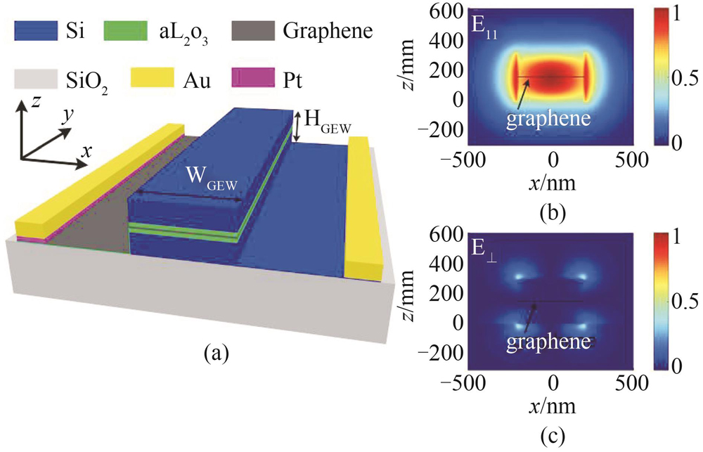
Fig. 1. (a)The schematic diagram of the GEW,(b)in-plane electric field distribution for TE mode,and(c)out-of-plane electric field distribution for TE mode
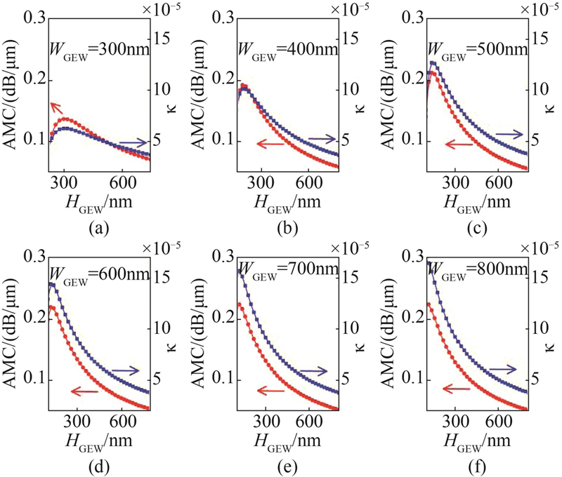
Fig. 2. The AMC(red circle)and
Fig. 3. The PMC(red circle)and
Fig. 4. (a)The schematic diagram of MZI based on optimized GEW(WGEW=800 nm,HGEW =100 nm),(b)Transmission of MZI based on the optimized GEW as a function of the applied voltage
Fig. 5. The real part of

Set citation alerts for the article
Please enter your email address
© Copyright 2018-2021 | Chinese Laser Press. All Rights Reserved 沪ICP备15018463号-20