A graphene-embedded waveguide (GEW) with improved modulation capability was proposed, which can be over 2 times larger than that of conventional graphene-on-silicon (GOS) waveguide. More importantly, it is found that the improvement of modulation capability mainly results from the enhanced electric field confinement around graphene. Based on this finding, we propose a high-efficient method to optimize the modulation capability. By using this method, the optimization work can be reduced by an order of magnitude. Our work may promote the design of graphene-based electro-optic modulator with high modulation capability.
In current integrated optoelectronic circuits,electro-optic modulator is an essential component performing electro-optic conversion. For the modulator based on electro-absorption(EA)effect,the modulation is realized by tuning the absorption of the waveguide. Hence,the performance of EA modulator depends on the change of propagation loss per unit length,i.e. the amplitude modulation capability(AMC). For the modulator based on electro-refraction(ER)effect,the modulation is realized by tuning the propagation phase to control the resonance [1-5] or the interference [6-7]of the light. Therefore,the performance of ER modulator depends on the change of propagation phase per unit length,i.e. the phase modulation capability(PMC). Nevertheless,the AMC and PMC of traditional silicon waveguide are quite small due to the weak EA effect and ER effect in silicon. Hence,a quite long silicon waveguide is required,e.g. a typical silicon modulator usually needs the length of ~1 mm[8]. Furthermore,it is not cost-efficient to integrate such a large silicon modulator in a chip.
In order to reduce the footprint of electro-optic modulator,the GOS waveguide modulator has been proposed due to its enhanced AMC(~ 0.07 dB/μm)and PMC(~1.1 deg/μm)[9]. However,it is found that the interaction between propagating light and graphene is relatively weak in the GOS waveguide modulator [10-15]. This is because most of the electric field is confined in the silicon waveguide and has little interaction with the top graphene layer [16-19].Therefore,the AMC and PMC can be improved further only if the electric field can be confined around graphene by using an elaborately designed waveguide modulator structure.
In this work,a GEW with improved AMC and PMC is proposed. The AMC and PMC of GEW can be 3 and 2 times larger than those of traditional GOS waveguide respectively. The improvement is achieved by enhancing the electric field confinement around graphene. As a result,the footprint of the modulator based on GEW can be more compact than that based on GOS. Moreover,a high-efficient method to optimize the AMC and PMC of GEW is proposed. Based on this method,the optimization work can be cut down by an order of magnitude.
1 Structure
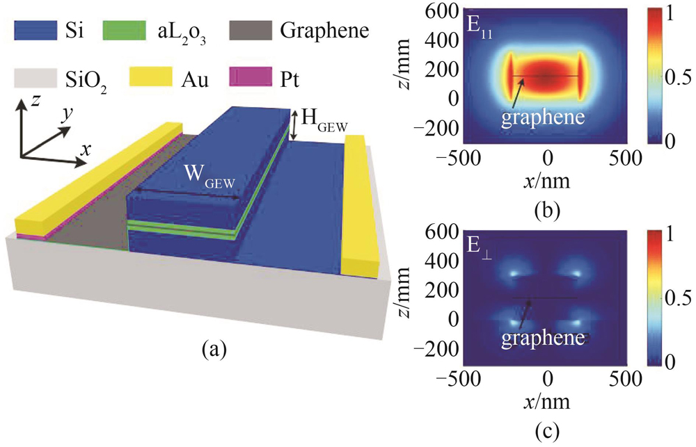
The structure of GEW is shown in Fig. 1(a). A silicon layer with a width of WGEW and a height of HGEW is on the silica substrate. Monolayer graphene is embedded into a 14-nm-thickness aluminum oxide layer which is in the center of silicon. Besides,graphene is modeled as anisotropic material shown as the Appendix. Its out-of-plane relative permittivity is fixed at 2.5 while its in-plane relative permittivity varies with chemical potential which can be tuned by external voltage [20](the detail can be found in the Appendix). By using the eigen mode analysis at optical communication wavelength 1550 nm,the transverse electric(TE)mode of GEW is shown in Fig. 1(b)(in-plane electric field intensity )and Fig. 1(c)(out-of-plane electric field intensity ).
Figure 1.(a)The schematic diagram of the GEW,(b)in-plane electric field distribution for TE mode,and(c)out-of-plane electric field distribution for TE mode
When the TE mode propagates along GEW,its loss per micron and phase change per micron can be expressed as
,
and
,
respectively,where is the wavelength, is the effective mode index of TE mode. Furthermore,the AMC and PMC of GEW can be expressed as
,
and
,
where is the change of effective mode index induced by the variation of . According to electromagnetic theory [21-22], can be approximated as
.
In Eq. 5,,,, and are the relative permittivity of Si,Al2O3,SiO2,air and graphene respectively. ,,, and are the electric field intensity inside the region of Si,Al2O3,SiO2,air and graphene respectively. ,,, and are the area for the region of Si,Al2O3,SiO2,air and graphene respectively. Because the on graphene is much smaller than the on graphene shown as Fig 1.(b)and Fig 1.(c). Therefore,the on graphene can be ignored,which means and can be approximated as and respectively. Hence, can be further expressed as
,
where, and. Because the electric field integration in graphene is much smaller than the sum of electric field integration in the whole waveguide, will approach 0. Based on the Taylor’s series expansion,the can be approximated as
.
Because of the ultrathin thickness of graphene,it is assumed that the variation of graphene permittivity nearly does not change the field distribution. Therefore, can be expressed as
.
By substituting Eq.8 into Eq.3 and Eq.4,the AMC and PMC can be expressed as
,
and
,
respectively. Since most of the electric field is in the silicon region, is estimated to be near the refractive index of silicon. According to Eqs. 9-10,it is found that the modulation capability(MC)including AMC and PMC mainly depends on the normalized changeable electric displacement field ,i.e. the ratio of the changed electric displacement field caused by graphene to the electric displacement field in the whole waveguide except graphene. Hence,the AMC and PMC can be improved by enlarging the factor ,which means the electric field needs to be confined in graphene region as much as possible.
3 Optimization
In order to optimize the AMC and PMC of GEW,a sweep of the geometrical parameters including the waveguide height HGEW and the chemical potential of graphene under different waveguide width WGEW is taken. In the following discussion,graphene is set to be at the center of silicon while sweeping HGEW ranging from 100 nm to 800 nm with an increase step of 20 nm and ranging from 0 eV to 1 eV with an increase step of 0.05 eV. The and field distribution are obtained from numerical simulation. Then the AMC,PMC and can be calculated with Eqs.3-4 and the equation ,respectively.
In traditional method,locally maximum AMC and PMC at each HGEW need to be found by sweeping [16-18]. By comparing these locally optimized AMC and PMC under different HGEW,the globally optimized AMC and PMC can be found. Therefore,the total sets of simulation will be =756,where M=36 is the number of HGEW and N=21 is the number of . However,this optimization strategy usually requires long simulation time and huge storage space.
In order to relieve the simulation burden,a high-efficient optimization method based on the physical understanding of MC is proposed. On the one hand,AMC and PMC mainly depend on and as Eqs.9-10 show. On the other hand, is mainly determined by and is mainly determined by electric field distribution varying with geometric parameters. Hence,the AMC and PMC can be optimized by sweeping and HGEW independently. First,M simulations are set under different HGEW(shown as the blue square in Fig. 2(a-f)or Fig. 3(a-f))to find the H*GEW where reaches its maximum. After fixing HGEW at H*GEW,N simulations are set under different to find the best AMC and PMC. Hence,the total sets of simulation are only =57. Comparing to traditional optimization method(=756),the simulation time and memory requirement can be cut down by at least 1 order of magnitude.
In Figs. 2(a-f),the AMC first increases with HGEW then decreases with HGEW. Meanwhile,the peak of AMC gradually moves to the point of smaller HGEW as WGEW increases. It is also found that the locally optimized AMC increases with WGEW but the increment will be smaller and smaller. At WGEW=800 nm and HGEW=100 nm,the globally optimized AMC is found to be ~0.224 dB/μm,which is over 3 times larger than the AMC of a typical GOS waveguide [9]. As a result,the length of the EA modulator based on the optimized GEW can be reduced over 67% accordingly.
Similar high-efficient optimization method can also be used to optimize the PMC as Figs. 3(a-f)shows. It is found that the best PMC=~2.66 deg/μm is also reached at WGEW=800 nm and =100 nm. The PMC of the optimized GEW is over 2 times larger than the PMC of the GOS waveguide [9]. In Fig. 4(a),a Mach-Zehnder interferometer(MZI)modulator based on the optimized GEW(WGEW=800 nm,HGEW=100 nm)is proposed. Its optical transmission is given as:
,
where L=100μm is length of interferometer arms, and are the of the two arms[9]. By fixing the applied voltage on the arm A as ~6.1 V and tuning the applied voltage on the arm B from ~6.1 V to ~1.9 V,the phase difference between two arms varies from to . Accordingly,the transmission of the MZI decreases from 94.8%(binary state “1”)to 1.3%(binary state “0”)shown as Fig. 4(b). However,the applied voltage to realize phase difference for the MZI based on GOS waveguide will be as large as ~32.0 V [9]. Hence,the MZI based on the optimized GEW can be more energy-efficient.
Figure 4.(a)The schematic diagram of MZI based on optimized GEW(WGEW=800 nm,HGEW =100 nm),(b)Transmission of MZI based on the optimized GEW as a function of the applied voltage
In order to improve the modulation efficiency further,the structure which can provide larger should be used. As reported in previous study [17],the can be enlarged significantly by using the plasmonic waveguide and the self-biased graphene stacks. Since larger means more electric field is confined in graphene,the AMC of a typical graphene modulator based on plasmonic waveguide can be increased to as large as 0.84 dB/μm [17]. However,a large optical loss of 0.09 dB/μm should be taken care of and a special coupler needs to be added,which may lead to a more complicated design [17].
4 Conclusion
In summary,the physical understanding for the modulation capability(including AMC and PMC)of GEW is provided in this paper. The normalized changeable electric displacement field is found to be the main determining factor for the modulation capability. Based on this finding,a high-efficient method to optimize the modulation capability is proposed. By using the proposed optimization method instead of traditional method,the simulation time and storage space can be cut down by at least 1 order of magnitude. After optimization,the AMC or PMC of GEW can be over 3 or 2 times larger than those of a typical GOS waveguide respectively. Hence,a more compact or energy-efficient modulator can be achieved. This work may pave the way for designing graphene-based electro-optic modulator with large modulation capability.
Here,graphene is modeled as an anisotropic material. Its out-of-plane relative permittivity is 2.5 and in-plane relative permittivity is
,
where is the surface conductivity of graphene, is the angular frequency,=0.34 nm is the thickness of graphene and is the permittivity in free space [23]. Based on Kubo formula, can be calculated as
,
where is the charge of electron, is the reduced Planck’s constant, is the scattering rate and is the Fermi-Dirac function [24]. Furthermore, can be expressed as
,
where is the chemical potential of graphene, is the Boltzmann constant and =300 K is the temperature [23]. Moreover, can be controlled by the external voltage:
,
where is estimated with a parallel-plate capacitor model, is the Fermi velocity, is the driven voltage and is the voltage offset due to natural doping [25]. For simplicity but not losing principle, can be considered as the applied voltage on graphene.
According to Eqs.12-15,it is found that the can be modified by varying ,which can be further tuned by changing the applied voltage shown as Fig. 5.
Figure 5.The real part of (green triangle),the imaginary part of (red square)and the chemical potential of graphene (blue circle)
[6] R G CHEN, R LIN, L M SHEN et al. 3-μm mid-infrared polarization-independent and CMOS-compatible graphene modulator. Journal of Infrared and Millimeter Waves, 40, 297(2021).
[14] Z Cheng, X Zhu, M Galili et al. Double-layer graphene on photonic crystal waveguide electro-absorption modulator with 12 GHz bandwidth. Nanophotonics, 9, 2377-85(2020).