
Khant Minn, Blake Birmingham, Brian Ko, Ho Wai Howard Lee, Zhenrong Zhang. Interfacing photonic crystal fiber with a metallic nanoantenna for enhanced light nanofocusing[J]. Photonics Research, 2021, 9(2): 252
- Photonics Research
- Vol. 9, Issue 2, 252 (2021)
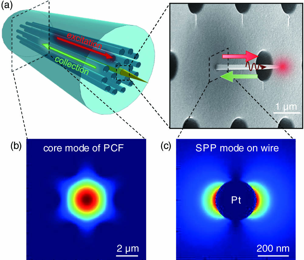
Fig. 1. PCF-nanoantenna hybrid probe. (a) Schematics of the device. (b) Simulated intensity profile of fundamental guided mode in the PCF at 560 nm wavelength. (c) Simulated intensity profile of HE 11
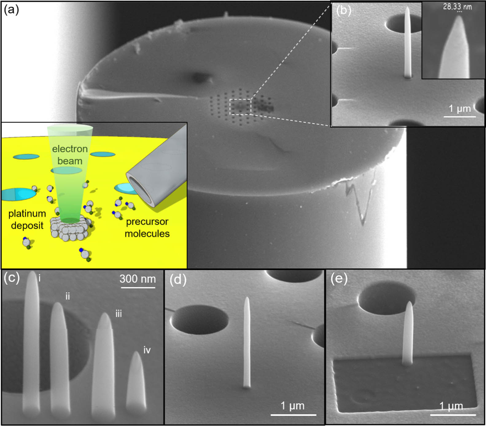
Fig. 2. Device fabrication with electron-beam-induced deposition (EBID). (a) Schematics of the EBID process and overview SEM image of PCF. (b)–(e) SEM images of the fabricated samples on PCFs taken at 52 degrees inclination. The deposition parameters, base diameter, and height of each tip are tabulated in the Methods section.
Fig. 3. Fiber coupling and the polarization-resolved imaging of side-scattered light. (a) Schematic of the optical setup. (b) Illustration of SPP vector components along the tip. (c)–(f) Optical images of the side scattering from the tip when the output polarizer is (c), (e) along the tip axis (longitudinal), and (d), (f) perpendicular to the tip axis (transverse). (c), (d) Taken with 530 nm filter. (e), (f) Taken with 630 nm filter. The dashed lines are the visual guide for outline of the PCF. The bottom panel is the SEM image overlaid on the optical image.
Fig. 4. Effect of rectangular aperture on mode coupling. (a) The electric field intensity profile of the aperture-tip geometry. (b) Propagation along the tip producing nanofocusing at the apex for x y
Fig. 5. Side-scattering from the PCF-aperture-antenna system. (a)–(d) Optical images of the side scattering from the tip when the input polarizer is parallel to the gap between the tip and aperture wall, with the output polarizer (a), (c) along the tip axis (longitudinal), and (b), (d) perpendicular to the tip axis (transverse). The tip is present in (a) and (b), while it is absent in (c) and (d). (e)–(h) Scattering from the tip when the input polarizer is perpendicular to the gap between the tip and aperture wall, with the output polarizer (e), (g) along the tip axis and (f), (h) perpendicular to the tip axis. The tip is present in (e) and (f), while it is absent in (g) and (h). Scale bar: 10 μm is for all optical images. The green arrows in the SEM images of the samples on the left panel indicate the orientation of input polarization in the plane of the aperture.
|
Table 1. EBID Deposition Parameters and Corresponding Tip Dimensions

Set citation alerts for the article
Please enter your email address
© Copyright 2018-2021 | Chinese Laser Press. All Rights Reserved 沪ICP备15018463号-20