Abstract
The direct interfacing of photonic crystal fiber to a metallic nanoantenna has widespread application in nanoscale imaging, optical lithography, nanoscale lasers, quantum communication, in vivo sensing, and medical surgery. We report on the fabrication of a needle-shaped plasmonic nanoantenna on the end facet of a photonic crystal fiber using electron-beam-induced evaporation of platinum. We demonstrate the coupling of light from the fiber waveguide mode to the subwavelength nanoantenna plasmonic mode focusing down to the apex of the plasmonic needle using a polarization-resolved far-field side-scatter imaging technique. Our work provides an important step toward widespread application of optical fibers in nearfield spectroscopic techniques such as tip-enhanced Raman and fluorescence microscopy, single-photon excitation and quantum sensors, nanoscale optical lithography, and lab-on-fiber devices.1. INTRODUCTION
Optical fibers are the most broadly used optical waveguides and are essential components of broadband telecommunication. Efforts to expand their application beyond telecommunication have resulted in various fiber-based devices, including fiber lasers/nonlinear optics [1,2], biosensing and chemical sensing [3,4], optoelectronics [5], and in-fiber near-field imaging [6,7]. On the other hand, surface plasmon polariton (SPP) waveguides have been studied extensively and have many applications in controlling and confining light in the nanometer scale such as plasmonic circuits [8], tip-enhanced Raman spectroscopy [9], nanoscale ultrafast spectroscopy [10], and quantum optics [11]. However, the propagation distance in plasmonic waveguide is largely hindered by the optical absorption by metals at the visible and near-infrared regime. Thus, efficient coupling of low-loss photonic waveguide modes to the confined surface plasmon polariton and vice versa is necessary for practical plasmonic devices. To this end, plasmonic antennae and waveguides have been integrated with optical fibers in a number of configurations such as evanescent coupling of parallel waveguides [12–15], end-fire coupling [16,17], tapered fiber to metallic nanotaper [18,19], and aperture-assisted coupling [20,21], achieving micro- to nanoscale light transport due to the adiabatic nanofocusing of SPPs. In those studies, integration of nanometer-sized antenna onto a micrometer-sized fiber is a fairly involved process with multistep procedures such as pressure-assisted high-temperature melt filling of metal inside the holey optical fiber followed by splicing/cleaving [12], fiber tapering and metal coating, chemical synthesis of nanowires followed by micromanipulation to form contact [13,19], and electron-beam-assisted forming of “contamination tip” on tapered fiber followed by metal coating [20]; yet, precise control of the position and size of the antenna is difficult due to the ad hoc nature of the processes.
In this work, we report a simple and straightforward way of coupling a photonic to plasmonic waveguide mode, overcoming the difficulties mentioned above. Precise control of the position and size of the plasmonic antenna is achieved by directly writing a nanoscale metallic tip on fiber in a single step inside a focused-ion and scanning electron microscope (FIB-SEM) chamber, allowing for any fiber-antenna coupling configuration to be realized with high precision, in addition to the high yield of a designer 3D antenna with nanometer resolution. Our device can be described as a hybrid fiber-plasmonic probe, a coupled system of photonic crystal fiber (PCF) and metallic nanoantenna. A needle-like plasmonic nanoantenna is fabricated on the end facet of a PCF, as shown in Fig. 1(a). The fundamental core mode of the PCF [Fig. 1(b)] is propagated through the fiber and coupled to the SPP mode on the platinum nanoantenna [Fig. 1(c)] via end-fire coupling. Such direct coupling relaxes the phase-matching requirement, enables broadband coupling, and reduces propagation losses [16]. The coupled SPPs then propagate along the antenna toward the tapered end, where they converge to produce an enhanced and confined field at the nanoscale apex.
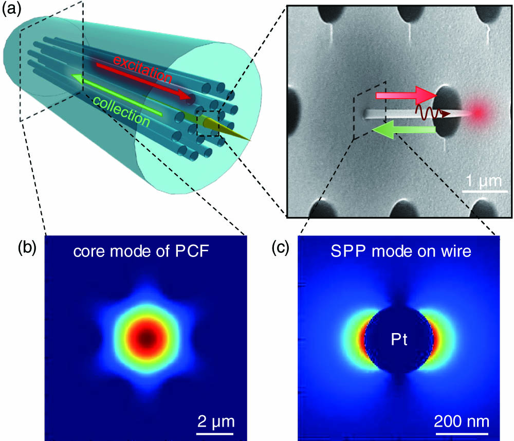
Figure 1.PCF-nanoantenna hybrid probe. (a) Schematics of the device. (b) Simulated intensity profile of fundamental guided mode in the PCF at 560 nm wavelength. (c) Simulated intensity profile of mode on a metallic nanowire waveguide at the same wavelength.
2. RESULTS AND DISCUSSIONS
To confirm the practicality of our device, we fabricate a platinum tip on the end facet of the PCF using electron-beam-induced deposition (EBID), a direct-writing technique capable of creating 3D complex structures with high-resolution [22,23]. The PCF is chosen over the step-index fiber because of single-mode transmission over a broad bandwidth covering the visible and near-infrared [24]. The modal confinement of PCF can be designed as small as for efficient coupling. Moreover, the presence of air-hole cladding makes it easier to align the plasmonic antenna in the core during fabrication. In this technique, metallo-organic precursor gas is introduced near the surface of the PCF facet through the injection nozzle, as shown in the inset of Fig. 2(a). The PCF facet is precoated with a thin layer of gold to avoid charging (see Methods section for details). Then, the focused electron beam is scanned over a circular area. When the electron beam interacts with the gas, the volatile organic molecules evaporate, and the metal part is adsorbed on the surface forming a thin metal disc [22,25]. The structure becomes taller with an increasing number of passes. At the same time, deposited metal at each new pass spills over the edge, resulting in the cone-shaped tip formation at the top of the structures. This process is repeated until a conical pillar with the desired height is formed. The width of the deposited structure is slightly larger than the electron beam scan area. Primary electrons scattering and outgoing secondary emissions occur over an area much larger than the beam spot size [26]. Therefore, the smallest width is limited by the resolution of the scan area. Nanowires with different lengths and diameters have been fabricated for this study. The SEM images of some of the fabricated tips are shown in Figs. 2(b)–2(e). The inset of Fig. 2(b) shows a high-resolution SEM image of the tip apex. The radius of curvature at the tip apex is less than 14 nm. The tip radius of our fabricated samples ranges from about 14 to 40 nm. The tip radius of the sample in Fig. 2(d) is about 19 nm and is 26 nm in Fig. 2(e). Details of the fabrication parameters and the sizes of the tips can be found in the Methods section. Results from optical measurements of the two samples in Figs. 2(d)and 2(e) are discussed below.
Sign up for Photonics Research TOC. Get the latest issue of Photonics Research delivered right to you!Sign up now

Figure 2.Device fabrication with electron-beam-induced deposition (EBID). (a) Schematics of the EBID process and overview SEM image of PCF. (b)–(e) SEM images of the fabricated samples on PCFs taken at 52 degrees inclination. The deposition parameters, base diameter, and height of each tip are tabulated in the Methods section.
To demonstrate the light coupling and focusing performance of our nanoprobe device, we chose a representative tip among the fabricated samples. It has a height of 2.353 μm and diameter of 164 nm at the center of a PCF with a 5 μm core diameter [Fig. 2(d)]. A 30 nm thick gold layer is coated on the PCF to avoid charging during the nanowire fabrication while allowing light to be transmitted through the fiber end. We performed optical characterization of the fabricated tip by imaging the scattered light to the side of the tip. The side-scattered light is imaged in the far-field using the setup illustrated in Fig. 3(a). The light source from the supercontinuum laser is free space coupled to the bare end of the PCF. At the other end with the plasmonic tip, an objective ( magnification and 0.9 NA) is placed to collect the light scattered to the side of the tip to be imaged on the charge-coupled device (CCD) after going through a polarizer and a bandpass filter having 10 nm full width at half maximum centered at 530 and 630 nm. For the sample shown in Fig. 3, input power of 402 mW is used and 10 mW for the sample (see details in Fig. 5). Most of the tips were not damaged at low input power, confirmed by inspecting with SEM. The tip (shown in Fig. 5) is found to withstand up to 240 mW.
Figure 3.Fiber coupling and the polarization-resolved imaging of side-scattered light. (a) Schematic of the optical setup. (b) Illustration of SPP vector components along the tip. (c)–(f) Optical images of the side scattering from the tip when the output polarizer is (c), (e) along the tip axis (longitudinal), and (d), (f) perpendicular to the tip axis (transverse). (c), (d) Taken with 530 nm filter. (e), (f) Taken with 630 nm filter. The dashed lines are the visual guide for outline of the PCF. The bottom panel is the SEM image overlaid on the optical image.
Figure 4.Effect of rectangular aperture on mode coupling. (a) The electric field intensity profile of the aperture-tip geometry. (b) Propagation along the tip producing nanofocusing at the apex for -polarized light. The color bar represents the field intensity normalized with respect to excitation intensity. Inset: focusing efficiency as a function of wavelength. (c), (d) Same as (a), (b) but for -polarization with fields canceling near the apex. The green arrows in (a) and (c) indicate the input polarization.
Figure 5.Side-scattering from the PCF-aperture-antenna system. (a)–(d) Optical images of the side scattering from the tip when the input polarizer is parallel to the gap between the tip and aperture wall, with the output polarizer (a), (c) along the tip axis (longitudinal), and (b), (d) perpendicular to the tip axis (transverse). The tip is present in (a) and (b), while it is absent in (c) and (d). (e)–(h) Scattering from the tip when the input polarizer is perpendicular to the gap between the tip and aperture wall, with the output polarizer (e), (g) along the tip axis and (f), (h) perpendicular to the tip axis. The tip is present in (e) and (f), while it is absent in (g) and (h). Scale bar: 10 μm is for all optical images. The green arrows in the SEM images of the samples on the left panel indicate the orientation of input polarization in the plane of the aperture.
The excitation of SPPs on the tip can be verified by analyzing the polarization of light that scatters to the side of the tip. In Figs. 3(c) and 3(e), when the output polarization analyzer is oriented along the antenna axis to collect the longitudinal component of scattered SPP, the intensity is much larger than in the case when the analyzer is oriented perpendicularly to the antenna axis [Figs. 3(d) and 3(f)] to collect the transverse component. The linearly polarized PCF core mode cannot efficiently excite the radially symmetric SPP (TM01) mode on the metal tip because of the modal field mismatch. The first-order SPP (HE11) mode polarized along the axis exhibits antisymmetric electric field distribution about the axis [27,28] and can be excited with the linearly polarized incident core mode from PCF. However, at the mode cut-off radius, when the effective index of the mode approaches the index of air, it couples to the far-field radiation and thus could not focus down to the apex of the nanowire [28,29]. In this case, we expect to see stronger scattering of a transverse than a longitudinal component, as depicted in Fig. 3(b). However, with a small asymmetry in the shape of the tip such as a slight tilt, phase difference between the two counterpropagating modes of the tip could be introduced, allowing a portion of the optical energy to be coupled to the radially symmetric SPP () mode [21,30]. The tapered geometry of the tip forces the radial SPP to slow down and asymptotically converge toward the apex [31]. As they do, the longitudinal component of the SPP becomes larger, and the transverse component is suppressed. As a result, the light that is scattered to the side from the apex has a mostly longitudinal component. Evidently, the side-scattered light is composed mainly of longitudinal components, as shown in Figs. 3(c) and 3(e), suggesting that the SPPs are focused near the tip apex where they scatter to the far field. However, there still exists a transverse component in the scattered light, as shown in Figs. 3(d) and 3(f), which implies that the SPPs scatter before they reach the apex. To avoid coupling to the leaky mode and improve the asymmetrical coupling of the linearly polarized light with the tip, we modify the coupling conditions at the fiber-tip interface by introducing a metallic aperture close to the nanowire.
To improve the focusing efficiency of the device, we fabricate a probe with a rectangular aperture at the tip-PCF interface. In this device, PCF is coated with 100 nm Au to block the transmitted light. A aperture is milled with a focused-ion beam at the center of the core. Afterward, the tip is fabricated inside the aperture next to one of the long edges of the aperture, as shown in Fig. 2(e). The modes supported by the aperture and tip system are calculated by the finite element method and plotted in Fig. 4. In Fig. 4(a), the input polarization is parallel to the gap between the tip and the edge of the aperture, which we refer to as polarization for simplicity. The aperture shifts the spatial distribution of electromagnetic fields, which are coupled to the tip, mostly to the exposed side, i.e., the side that opens out to the center of the core. On the side that forms a gap with the wall of the aperture, the field does not couple to the SPP. This asymmetric or one-sided coupling of SPPs on the tip evolves to radial SPPs, which can propagate to the apex, resulting in nanofocusing, as shown in Fig. 4(b). It shows the intensity enhancement factor of about 24 at the tip apex compared with the fiber core. The inset of Fig. 4(b) shows the focusing efficiency for -polarization, defined as the ratio of the electric field intensity integrated over a small region at the apex above the tip surface extending 10 nm into air with respect to the same quantity inside the core of the excitation fiber. The efficiency in the near-infrared is about 2.3%, while it is about 0.1% in the visible. The low efficiency in the visible is due to the lossy nature of Pt and can be improved by using Au or Ag as the plasmonic tip material as well as tip size. The nanofocusing via asymmetric coupling has been thoroughly investigated theoretically and reported by our group in the previous study [21]. In Fig. 4(c), the input polarization is perpendicular to the gap between the tip and the aperture wall, which we refer to as -polarization. In this case, distribution of the SPP modal field around the tip remains antisymmetric about the axis. As they propagate toward the narrowing tip, they destructively interfere with each other, and no enhancement results at the apex as shown in Fig. 4(d).
Figures 5(a) and 5(b), respectively show the measured optical image of side-scattered longitudinal and transverse components from the aperture-antenna when the input is -polarized. In this polarization, the asymmetric mode discussed in Fig. 4(a) is excited at the tip base and SPPs can focus on the apex. From the images, the side-scattered light is seen to be purely longitudinally polarized, implying that it originates from focused SPPs. To confirm that the strong longitudinal scattering is solely from the tip and not from the aperture edges, we prepare a control PCF sample with only an aperture. When the tip is absent, as shown in Figs. 5(c) and 5(d), the scattering from the aperture has a weaker longitudinal component than transverse in addition to having a large spatial extent, confirming that the scattering of longitudinal components in Fig. 5(a) is from the tip, not from the aperture. We note that scattering from the aperture has a stronger transverse component because the input -polarization aligns with the transverse orientation of the output.
Next, we rotate the input polarization by 90 degrees so that the PCF mode is -polarized. At the fiber-tip interface, the fiber core mode couples to the -polarized antisymmetric SPP mode, as shown in Figs. 4(c) and 4(d). As such, the coupled SPPs on the opposing sides of the tip destructively interfere with each other as the tip radius narrows and scattering occurs without focusing at the apex. As a result, the longitudinal component is weaker than the transverse, as shown in the side-scattering images in Figs. 5(e) and 5(f). In contrast to Figs. 3(c)–3(f), where an accidental tilt of the tip is invoked to justify the experimental results, the introduction of an aperture allows us to confirm the SPP focusing via control of the input polarization. For the control sample with aperture only, it is seen in Figs. 5(g) and 5(h) that the scattered light from the aperture has a stronger longitudinal component than the transverse, confirming that the scattering in Fig. 5(f) is from the tip and not from the aperture. We again note that, when the incident beam from PCF is -polarized, the light that is scattered from the aperture toward the detector is polarized along the plane. Thus, the detected light contains a more longitudinal (-polarized) component than transverse (-polarized).
The demonstrated input-polarization selectiveness of the device shows that the aperture clearly modified the light coupled to the plasmonic tip. For -polarized input, the light scattered from the tip contains no transverse component, indicating higher focusing performance. The aperture and tip parameters such as the width, height, and gap size, can be optimized to further increase the coupling and focusing efficiencies as well as the suppression of background scattering from the fiber core. In our previous work employing similar coupling mechanism, we reported 136-fold field enhancement and 1.3% focusing efficiency [21], which is better than or comparable with the performance of existing nearfield probes [32–34]. The PCF core size is also an important factor that determines the focusing efficiency. Since the modal field overlap between the core mode and the nanowire plasmonic mode determines the coupling efficiency in the end-fire coupling scheme, the core diameter should be at least in the same order of magnitude as the nanowire diameter. On the other hand, as core size becomes smaller, the free space coupling loss into the fiber as well as the attenuation along the fiber becomes large. In this work, we use the smallest commercially available core size PCF that has low attenuation over a broad bandwidth. Metals with larger real part of permittivity and less absorption than platinum such as gold and silver can also be used as the tip material for improved performance; however, the precursor for those metals often results in residual carbon impurity during deposition; thus, Pt is preferred for applications related to FIB-SEM machining. Alternatively, a thin layer () of Au or Ag can be deposited on the Pt tips by sputtering or evaporation techniques to mitigate the losses of Pt, but the optimization of the device is beyond the scope of the current study. We believe that, with judicious choice of the parameters mentioned above, our device provides a unique and efficient tool to study nanoscale light–matter interaction such as fiber-based tip-enhanced Raman and fluorescence spectroscopies.
3. CONCLUSIONS
We demonstrate a photonic-plasmonic probe employing a straightforward excitation scheme that couples linearly polarized light from the optical fiber to nanofocusing plasmons on the plasmonic tip aided by an aperture at the fiber-tip interface. As a proof of concept, PCF-nanoantenna probes are fabricated and optically characterized. We showed that, when the input polarization is in the direction where aperture-tip geometry is asymmetric, the scattered light from the antenna is longitudinally polarized, which confirms the plasmonic coupling and nanofocusing. Our probe is a promising platform for the development of novel devices and applications such as remote sensing and nearfield spectroscopes, single photon excitation and quantum sensors, nanoscale optical lithography, and lab-on-fiber devices.
4. METHODS
A. Numerical Simulation
Numerical simulations of the photonic-plasmonic probe were carried out using the MODE Solutions and FDTD Solutions software from Lumerical Solutions, Inc. The permittivity function of silica and platinum is modeled with a multicoefficient function fitted to the Palik data [35] and gold Johnson and Christy data [36]. The PCF is modeled as a hexagonal lattice (lattice constant 3 µm) of air holes (diameter 1.25 µm) in a silica core with one defect at the center. A mesh size of 2 nm is employed in the region encompassing the tip for optimal convergence results.
B. Tip Fabrication
One end of the PCF (PMA-LM-5 from Thorlabs Inc.) is mechanically cleaved to have a clean and flat end surface, which is then coated with 30 nm thick gold layer for the sample in Fig. 3 and 100 nm for the one in Fig. 5 using magnetron sputtering. Then, the gold-coated PCF is loaded into the microscope chamber vertically. Depositions were performed in a focused-ion and electron beam system (Versa 3D from FEI Company). The acceleration voltage of 30 kV and beam current of 140 pA are used. Platinum precursor gas [trimethyl((1,2,3,4,5-eta)-1-methyl-2,4-cyclopentadien-1-yl)-platinum] is injected into the vacuum chamber near the fiber. The e-beam exposure begins when the chamber pressure stabilizes around (1 mbar = 100 Pa).
The physical dimensions of the tip, such as height and width, can be adjusted by controlling the dwell time and number of passes. In Table 1, we list the deposition parameters and the resulting physical dimension of a few of the fabricated tips. By changing the scan diameter, which is the diameter of the circular area over which the focused e-beam is scanned during deposition, from 75 to 300 nm, the base diameter of the tip is tuned from 150 to 540 nm (only the scan diameters up to 100 nm and tip base diameters up to 241 nm are listed in Table 1). The height of the tip can be tuned by varying the number of passes, but special care needs to be taken since the increasing passes will also widen the tip. For optimal resolution and aspect ratio, a small e-beam current of 140 pA and short dwell time are used, resulting in a large number of passes (). A dwell time of 2 μs results in a higher aspect ratio than dwell time of 1 μs. To show the reproducibility of our fabrication technique, five tips are fabricated using the same deposition parameters as the tip in Fig. 2(e). The standard deviation of the resulting tips’ base diameter is 10 nm (or 5% of the mean) and height 200 nm (or 10% of the mean).
| Scan Diameter (nm) | Dwell Time (µs) | Passes | Total Time (s) | Base Diameter (nm) | Height (µm) | Corresponding Figure |
|---|
| 75 | 1 | 1,343,069 | 32 | 167 | 0.950 | Fig. 2(c), iii |
| 75 | 1 | 2,166,241 | 52 | 146 | 1.263 | Fig. 2(c), i |
| 75 | 1 | 4,332,482 | 104 | 164 | 2.353 | Fig. 2(d) |
| 100 | 1 | 4,332,482 | 13 | 173 | 0.561 | Fig. 2(c), iv |
| 100 | 1 | 1,083,121 | 32 | 190 | 1.098 | Fig. 2(c), ii |
| 100 | 2 | 1,126,445 | 65 | 216 | 1.060 | |
| 100 | 2 | 1,689,668 | 98 | 241 | 1.610 | Fig. 2(e) |
| 100 | 2 | 2,166,241 | 126 | 237 | 1.953 | |
Table 1. EBID Deposition Parameters and Corresponding Tip Dimensions
Acknowledgment
Acknowledgment. The authors acknowledge the support of the Center for Microscopy and Imaging as well as support for usage of the Kodiak high-performance computing cluster at Baylor University.
References
[1] R. H. Stolen, H. W. K. Tom. Self-organized phase-matched harmonic generation in optical fibers. Opt. Lett., 12, 585-587(1987).
[2] N. Granzow, S. P. Stark, M. A. Schmidt, A. Tverjanovich, L. Wondraczek, P. St. J. Russell. Supercontinuum generation in chalcogenide-silica step-index fibers. Opt. Express, 19, 21003-21010(2011).
[3] C. Caucheteur, T. Guo, J. Albert. Review of plasmonic fiber optic biochemical sensors: improving the limit of detection. Anal. Bioanal. Chem., 407, 3883-3897(2015).
[4] S. E. Mowbray, A. M. Amiri. A brief overview of medical fiber optic biosensors and techniques in the modification for enhanced sensing ability. Diagnostics, 9, 23(2019).
[5] M. Bayindir, F. Sorin, A. F. Abouraddy, J. Viens, S. D. Hart, J. D. Joannopoulos, Y. Fink. Metal–insulator–semiconductor optoelectronic fibres. Nature, 431, 826-829(2004).
[6] M. Mivelle, T. S. van Zanten, M. F. Garcia-Parajo. Hybrid photonic antennas for subnanometer multicolor localization and nanoimaging of single molecules. Nano Lett., 14, 4895-4900(2014).
[7] K. Minn, B. Birmingham, Z. Zhang. New development of nanoscale spectroscopy using scanning probe microscope. J. Vac. Sci. Technol. A, 38, 030801(2020).
[8] R. W. Heeres, L. P. Kouwenhoven, V. Zwiller. Quantum interference in plasmonic circuits. Nat. Nanotechnol., 8, 719-722(2013).
[9] X. Ma, Y. Zhu, N. Yu, S. Kim, Q. Liu, L. Apontti, D. Xu, R. Yan, M. Liu. Toward high-contrast atomic force microscopy-tip-enhanced Raman spectroscopy imaging: nanoantenna-mediated remote-excitation on sharp-tip silver nanowire probes. Nano Lett., 19, 100-107(2019).
[10] S. Berweger, J. M. Atkin, R. L. Olmon, M. B. Raschke. Light on the tip of a needle: plasmonic nanofocusing for spectroscopy on the nanoscale. J. Phys. Chem. Lett., 3, 945-952(2012).
[11] Z.-K. Zhou, J. Liu, Y. Bao, L. Wu, C. E. Png, X.-H. Wang, C.-W. Qiu. Quantum plasmonics get applied. Prog. Quantum Electron., 65, 1-20(2019).
[12] H. W. Lee, M. A. Schmidt, H. K. Tyagi, L. P. Sempere, P. St. J. Russell. Polarization-dependent coupling to plasmon modes on submicron gold wire in photonic crystal fiber. Appl. Phys. Lett., 93, 111102(2008).
[13] X. Guo, M. Qiu, J. Bao, B. J. Wiley, Q. Yang, X. Zhang, Y. Ma, H. Yu, L. Tong. Direct coupling of plasmonic and photonic nanowires for hybrid nanophotonic components and circuits. Nano Lett., 9, 4515-4519(2009).
[14] H. W. Lee, M. A. Schmidt, R. F. Russell, N. Y. Joly, H. K. Tyagi, P. Uebel, P. St. J. Russell. Pressure-assisted melt-filling and optical characterization of Au nano-wires in microstructured fibers. Opt. Express, 19, 12180-12189(2011).
[15] H. W. Lee, M. A. Schmidt, P. St. J. Russell. Excitation of a nanowire “molecule” in gold-filled photonic crystal fiber. Opt. Lett., 37, 2946-2948(2012).
[16] X.-W. Chen, V. Sandoghdar, M. Agio. Highly efficient interfacing of guided plasmons and photons in nanowires. Nano Lett., 9, 3756-3761(2009).
[17] A. Tuniz, M. A. Schmidt. Interfacing optical fibers with plasmonic nanoconcentrators. Nanophotonics, 7, 1279-1298(2018).
[18] X. Li, W. Li, X. Guo, J. Lou, L. Tong. All-fiber hybrid photon-plasmon circuits: integrating nanowire plasmonics with fiber optics. Opt. Express, 21, 15698-15705(2013).
[19] S. Kim, N. Yu, X. Ma, Y. Zhu, Q. Liu, M. Liu, R. Yan. High external-efficiency nanofocusing for lens-free near-field optical nanoscopy. Nat. Photonics, 13, 636-643(2019).
[20] H. G. Frey, F. Keilmann, A. Kriele, R. Guckenberger. Enhancing the resolution of scanning near-field optical microscopy by a metal tip grown on an aperture probe. Appl. Phys. Lett., 81, 5030-5032(2002).
[21] K. Minn, H. W. Howard Lee, Z. Zhang. Enhanced subwavelength coupling and nano-focusing with optical fiber-plasmonic hybrid probe. Opt. Express, 27, 38098-38108(2019).
[22] H. W. P. Koops, R. Weiel, D. P. Kern, T. H. Baum. High-resolution electron-beam induced deposition. J. Vac. Sci. Technol. B, 6, 477-481(1988).
[23] M. Huth, F. Porrati, O. V. Dobrovolskiy. Focused electron beam induced deposition meets materials science. Microelectron. Eng., 185-186, 9-28(2018).
[24] T. A. Birks, J. C. Knight, P. St. J. Russell. Endlessly single-mode photonic crystal fiber. Opt. Lett., 22, 961-963(1997).
[25] G. C. Gazzadi, S. Frabboni, C. Menozzi. Suspended nanostructures grown by electron beam-induced deposition of Pt and TEOS precursors. Nanotechnology, 18, 445709(2007).
[26] N. Silvis-Cividjian, C. W. Hagen, P. Kruit. Spatial resolution limits in electron-beam-induced deposition. J. Appl. Phys., 98, 084905(2005).
[27] S. Zhang, H. Wei, K. Bao, U. Håkanson, N. J. Halas, P. Nordlander, H. Xu. Chiral surface plasmon polaritons on metallic nanowires. Phys. Rev. Lett., 107, 096801(2011).
[28] D. Pan, H. Wei, Z. Jia, H. Xu. Mode conversion of propagating surface plasmons in nanophotonic networks induced by structural symmetry breaking. Sci. Rep., 4, 4993(2014).
[29] D. E. Chang, A. S. Sørensen, P. R. Hemmer, M. D. Lukin. Strong coupling of single emitters to surface plasmons. Phys. Rev. B, 76, 035420(2007).
[30] N. T. Thu, K. Tanaka, M. Tanaka, D. N. Chien. Superfocusing of surface plasmon polaritons by metal-coated dielectric probe of tilted conical shape. J. Opt. Soc. Am. A, 30, 1113-1118(2013).
[31] M. I. Stockman. Nanofocusing of optical energy in tapered plasmonic waveguides. Phys. Rev. Lett., 93, 137404(2004).
[32] . AFM probes and accessories(2020).
[33] C. C. Neacsu, S. Berweger, R. L. Olmon, L. V. Saraf, C. Ropers, M. B. Raschke. Near-field localization in plasmonic superfocusing: a nanoemitter on a tip. Nano Lett., 10, 592-596(2010).
[34] A. Tuniz, M. Chemnitz, J. Dellith, S. Weidlich, M. A. Schmidt. Hybrid-mode-assisted long-distance excitation of short-range surface plasmons in a nanotip-enhanced step-index fiber. Nano Lett., 17, 631-637(2017).
[35] E. D. Palik. Handbook of Optical Constants of Solids(1998).
[36] P. B. Johnson, R. W. Christy. Optical constants of noble metals. Phys. Rev. B, 6, 4370-4379(1972).


