Abstract
Based on the traditional directional coupler, we proposed a scheme to design on-chip polarization beam splitters using an inverse design method. In our scheme, the coupling area of the designed devices are only . By manipulating the refractive index of the coupling region, the devices can work in C-band, L-band, O-band, or any other communication band. Different from conventional design methods, which need to adjust the design parameters artificially, if the initial conditions are determined, the proposed scheme can automatically adjust the design parameters of devices according to specific requirements. The simulation results show that the insertion losses of the designed polarization beam splitters can be less than 0.4 dB (0.35 dB) for TE (TM) mode at the wavelengths of 1310, 1550, and 1600 nm, and the extinction ratios are larger than 19.9 dB for the TE and TM modes at all three wavelengths. Besides, the extinction ratios of both polarization states are more than 14.5 dB within the wavelength range of 1286–1364 nm, 1497–1568 nm, and 1553–1634 nm. At the same time, the insertion losses are smaller than 0.46 dB.1. INTRODUCTION
Due to the ability to ensure ultracompact photonic integrated circuits (PICs) and the advantage of CMOS-compatible processing, the silicon-on-insulator (SOI) platform has drawn appreciable attention in the past few years. However, nanostructures based on the SOI platform usually show strong birefringence, which can cause undesired polarization-dependent mode dispersion. Hence, the devices that can manipulate the polarization state of light become a vital part of PICs. Many functional devices have been proposed for this reason, including polarization beam splitters (PBSs) [1–15], polarization rotators (PRs) [16,17], and polarizers [18,19]. As a typical polarization-handling device, structures like multimode interferometers (MMIs) [1,2], Mach–Zehnder interferometers (MZIs) [3], photonic crystal structures [4], hybrid plasmonic silicon waveguides (HPWs) [5,6], grating structures [7–10], and directional couplers (DCs) [11–14] have been employed to realize polarization splitting. Among those structures, DC-based PBSs are preferred because they are easy to design and usually provide a smaller footprint [11–14]. However, due to the underlying phase-matching principle of DCs, the performance of these devices is very sensitive to fabrication errors. To relax the constraint of the phase-matching condition, grating-based PBSs have been extensively studied [7–10]. For example, Zhang et al. experimentally demonstrated a PBS with an extinction ratio (ER) of more than 30 dB and an insertion loss (IL) less than 1 dB [9]. More importantly, the proposed PBS exhibits a high tolerance for manufacturing errors and a low sensitivity to the coupling length. Unfortunately, due to the lack of a full analytic theory, the design of grating-based PBSs is very complicated. Recently, based on the concept of free-form metamaterials, Shen et al. proposed a PBS with a footprint of only [19]. This kind of device is extremely robust to fabrication errors, but under the limitation of scattering, the bandwidth of ER greater than 10 dB is only 32 nm.
In this paper, based on the simple DC structure and the concept of “objective first” [20–23], we use the inverse design method [24–28] to design PBSs numerically. Compared to traditional design methods, which require a large amount of manual tuning, we can easily design PBSs according to specific demands. The only thing we need to do is to give proper initial conditions for the design process. Due to the ability to search for the full design space of target devices with arbitrary topologies [25], the designed devices can work in C-band, L-band, and even O-band. Here, we have designed a series of PBSs with a coupling area of only . The insertion losses of these devices can be less than 0.4 dB (0.35 dB) for the TE (TM) mode at three far apart isolated wavelengths (1310, 1550, and 1600 nm), and the extinction ratios are bigger than 19.9 dB for the TE and TM modes at all three wavelengths. When it comes to broadband situations, the ERs of the two polarization states are more than 14.50 dB within the wavelength range of 1286–1364 nm, 1497–1568 nm, and 1553–1634 nm. As we know, the full coupling length for the fundamental TE (TM) mode for a traditional DC varies with the wavelength due to modal dispersion [10]. Generally speaking, the DC-based PBSs that work in a shorter band have a bigger footprint, and the design process of these devices could be more complicated [10,29]. Here, benefiting from using the full design space, the ERs of the TE (TM) mode can still be kept higher than 15.48 dB (18.87 dB) and the ILs are lower than 0.46 dB (0.31 dB) when the operation wavelength is located at the O-band (1286–1364 nm). More than that, as long as it does not violate the principles of physics (the coupled-mode theory), we can theoretically design a PBS in any communication band without changing the size of the device.
2. DESIGN PROCESS AND RESULTS
Similar to traditional DCs, the presented PBSs are composed of two parallel straight waveguides and a rectangular coupling region, which is divided into pixel. The sides of these square pixels are 40 nm, giving a coupling area of [Fig. 1(b)]. To minimize the device size, as depicted in Fig. 1, we choose the widths of the straight waveguides to be 360 nm (9 pixels). To ensure our devices can be fabricated in a single lithography step, the heights of the waveguides also are set to be exactly like the coupling region; that is, 220 nm. And the 220-nm-thick Si layer is placed in the middle of the silica cladding layer, which has a height of 40 pixels (1.6 μm). By changing the refractive index of each pixel in the coupling region (to be silicon or silica), the devices can work in different target bands. In fact, in addition to the refractive index distribution, the material dispersion also has an impact on the characteristics of those devices [30,31]. In this paper, however, to simplify the optimization model and improve the optimization efficiency, we ignored the effect of material dispersion.
Sign up for Photonics Research TOC. Get the latest issue of Photonics Research delivered right to you!Sign up now
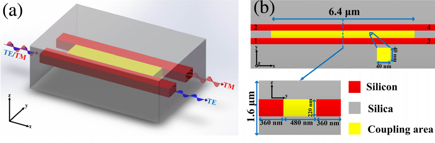
Figure 1.Schematic of the device. (a) Three-dimensional diagram. (b) Top view and side view. Fundamental TE mode and fundamental TM mode are coupled into the PBS from port 1, and after passing through the PBS, TE mode, and TM mode, are coupled out from port 3 and port 4, respectively.
Considering that the convergence of the inverse design method is determined by the “physics residuals” [20–23] of design objects, we start by giving proper initial conditions for the design process. For the structure described in Fig. 1, when the wavelength is specified, the effective indices of supported modes are uniquely determined by refractive indices of pixels in the cross section [yellow region in Fig. 1(b)]. The refractive indices can take the maximum value and the minimum value when all of the pixels in the cross section are occupied by silicon and silica, respectively [Fig. 2(a)]. According to the description of Section 3.2.1 in Ref. [30] and Section 4.3 in Ref. [31], the full coupling length (the length necessary for full power to transfer from one waveguide to the other, which is one-half of the beat length) of the fundamental mode is determined by the effective indices of the two first-order supermodes. Hence, the range of the full coupling length is determined by where and are the effective indices of two first-order supermodes . Figure 2(a) shows that there is an overlap between the value range of the effective indices of the TE0 (TM0) mode and the TE1 (TM1) mode [shaded parts of Fig. 2(a)], which means the extended maximum value of the full coupling length of the fundamental TE (TM) mode is infinity . Therefore, we cannot effectively estimate the maximum value of the full coupling length from Eq. (1). Fortunately, for the structure described in Fig. 1, with the increases of silicon composition in the cross section, the difference of the effective indices between the fundamental mode and the first-order mode will increase. Hence, the full coupling length will take the maximum value when the cross section of the coupling region is totally occupied by silica. In contrast to the maximum value, Fig. 2(a) clearly shows that the minimum value of the full coupling length can be calculated using . Figure 2(b) shows that the full coupling length of the TE mode can vary from 1.04 μm (black star) to 1539 μm (yellow star), but the full coupling length of the TM mode is limited in the scope of 1.98 μm (black triangle) to 206.5 μm (yellow triangle). This phenomenon can be simply explained. For the structure described in Fig. 1, the TE mode is mainly resonant in the x–y plane [10]; hence, changing the refractive index distribution will mainly affect the TE mode. Besides, we can see that both the maximum values of the TE mode and the TM mode rapidly increase when the wavelength decreases. In other words, it would be much more difficult to design a PBS in the O-band. Now the question is: how much of the coupling length should be taken? For a general inverse design problem, the design process is relatively simple. First, you specify the performance of the device by defining the conversion efficiency between the sets of input modes and output modes at several discrete frequencies. Second, use the “objective first” method and the steepest descent method to alternately update the field distribution and refractive index distribution until the “physics residuals” are lower than , or the upper limit of the iteration times has been satisfied [20–28].

Figure 2.(a) Maximum value and minimum value of the effective indices of different modes as a function of wavelength, where the shaded part represents the overlap between TE0 (TM0) and TE1 (TM1). (b) Full-coupling lengths of the fundamental TE (solid line) and TM (dotted line) modes as a function of wavelength, where the blue line represents the maximum value, the red line represents the minimum value, the yellow (black) star represents the maximum (minimum) value of TE mode, the yellow (black) triangle represents the maximum (minimum) value of TM mode, and the black dashed line represents the position of the wavelength of 1310 nm and 1550 nm, respectively.
To determine the size of the coupling region, we perform some tests at the wavelengths of 1310 nm and 1550 nm. As depicted in Fig. 1, the fundamental TE mode and the fundamental TM mode are coupled into the PBS devices from port 1, and, after passing through the PBS, TE mode, and TM mode, are coupled out from port 3 and port 4, respectively. During this design process, we specified that input power of the TE (TM) mode should be coupled out of port 3 (4) and less than 1% should be coupled out of port 4 (3). Figure 2(b) shows that the full coupling lengths of the TE and TM modes are in the range of 1.13 μm to 63.33 μm, and 2.08 μm to 11.49 μm (at the wavelength of 1550 nm). The information tells us that the minimum coupling length of the PBS is . Similarly, Fig. 2(b) also shows that the minimum coupling length is at the wavelength of 1310 nm. Therefore, if we want the device to achieve high performances at those two target wavelengths, the length of coupling region should be larger than 2.72 μm. Figure 3 shows the design results at the wavelengths of 1310 nm (solid line) and 1550 nm (dashed line), where the coupling lengths are chosen to be 1.4, 3.4, and 6.4 μm. As illustrated in Fig. 3, the performance (ERs and ILs) of the designed devices increases with the increasing of coupling length. The PBSs have poor performance when the coupling length is 1.4 μm (), but when the coupling length reaches 6.4 μm, the ERs of two polarization states can approach 20 dB and the ILs can be less than 0.4 dB at both wavelengths. Besides, Fig. 3 shows that the requested coupling length is inversely proportional to the wavelength. The coupling length of 3.4 μm is enough for a wavelength of 1550 nm, but the PBS requires a bigger coupling length (6.4 μm) at a wavelength of 1310 nm. The reason for this phenomenon is that the full-coupling length of the TE and TM modes is more sensitive to effective indices disturbance in a smaller wavelength range. As a result, a longer coupling length, which can provide more design freedom, is needed for a shorter wavelength. Here, to make sure the working wavelength can be expanded to C-band, L-band, and O-band, we choose the coupling length to be 6.4 μm.
Figure 3.Dependence of the performance of PBSs on coupling length, where the red (black) line and blue (green) line represent the power of TE (TM) modes to transmit to port 3 and port 4, respectively. To assure the convergence of the design process, the number of iterations is 300.
To illustrate the scalability of the proposed PBSs, except the two target wavelengths (1310 nm and 1550 nm) that have been described in Fig. 3, we choose another target wavelength (1600 nm), which belongs to the L-band. The geometry of the designed structure, the electric field amplitude distribution at the center of the devices, and the transmittance spectra of the three devices are shown in Fig. 4. As shown in Fig. 4, when the coupling length is chosen to be 6.4 μm, the inverse design method can realize polarization splitting at those three far apart target wavelengths, the ERs of the two polarization states can approach 20 dB (1%), and the ILs can be less than 0.4 dB (91.2%). Naturally, based on the conclusions of Figs. 3 and 4, we can predict that we can easily design PBS devices at any target wavelength (within the range of 1310–1600 nm).
Figure 4.Design results at the wavelengths of 1310, 1550, and 1600 nm. (a)–(c) Grayscale map of the designed structures, where white represents silica and black represents silicon. (d)–(f) The distribution of electric field amplitude at the center of the devices. (g)–(i) The broadband transmission of the designed devices, where the red (blue) solid line represents the transmission of the TE mode at port 4 (3) and the red (blue) dashed line represents the transmission of TM mode at port 4 (3). In addition, the double-sided black arrow represents the target wavelength. The coupling lengths are 6.4 μm.
The transmittance spectra in Figs. 4(i)–4(k) reveal that the device performance quickly drops off as one moves away from the target wavelength. To design broadband PBSs, we specified multiple target wavelengths in our design process that have identical desired performances (95% versus 1%). The geometry of the designed structures and the corresponding broadband operation spectra are shown in Figs. 5(a)–5(c) and Figs. 5(d)–5(f), respectively. Figure 5 reveals that the broadband operation has been achieved. As shown in Figs. 5(g)–5(i), under the limitation of (90%), the bandwidths of both polarization states are larger than 72 nm (1286–1364 nm, 1497–1568 nm, and 1553–1634 nm). At the same time, the ER can be larger than 14.5 dB (3.55%).
Figure 5.Design results at the wavelength ranges of 1290–1350 nm, 1510–1570 nm, and 1570–1630 nm. The distances between multiple target wavelengths are 20 nm, which gives a 60 nm design bandwidth for each device. (a)–(c) Grayscale map of the designed structures, where white represents silica and black represents silicon. (d)–(f) The broadband transmission of the designed devices, where the red (blue) solid line represents the transmission of TE mode at port 4 (3), the red (blue) dashed line represents the transmission of TM mode at port 4 (3), and the double-sided black arrows represent the target wavelengths. (g)–(i) The ERs and ILs of the designed devices, where the wavelengths of and are 1286–1364 nm, 1497–1568 nm, and 1553–1634 nm. The definitions of ER and IL are . For example, the ER and IL of TE mode are and , respectively. The coupling lengths are 6.4 μm.
3. CONCLUSION
In conclusion, we have numerically proposed a scheme to design on-chip polarization beam splitters. In our scheme, the footprints of the coupling regions are only . By manipulating the refractive index of a coupling region, the PBS devices can work in C-band, L-band, O-band, or any other communication band. The simulation results show that the insertion losses of the designed polarization beam splitters are less than 0.4 dB (0.35 dB) for TE (TM) mode at three wavelengths, and the extinction ratios are larger than 19.9 dB for the TE and TM modes. Besides, the extinction ratios of both polarization states are more than 14.5 dB within the wavelength ranges of 1286–1364 nm, 1497–1568 nm, and 1553–1634 nm. At the same time, the ILs are smaller than 0.46 dB. Our results indicate that the inverse design method can efficiently design high-performance PBS under the guidance of basic physics theory (the coupled-mode theory). In addition, this method can easily be applied to design most types of photonic devices. Unlike design methods such as the direct binary search (DBS) algorithm [19,32], the genetic algorithm [33,34], and the topology optimization method [35], which empirically give a design region (including shape and size), we proposed a semi-quantitative analysis method based on the coupled-mode theory to determine the size of the design region.
References
[1] B. M. A. Rahman, N. Somasiri, C. Themistos, K. T. V. Grattan. Design of optical polarization splitters in a single-section deeply etched MMI waveguide. Appl. Phys. B, 73, 613-618(2001).
[2] Y. Ding, H. Ou, C. Peucheret. Wideband polarization splitter and rotator with large fabrication tolerance and simple fabrication process. Opt. Lett., 38, 1227-1229(2013).
[3] L. M. Augustin, R. Hanfoug, J. J. G. M. van der Tol, W. J. M. de Laat, M. K. Smit. A compact integrated polarization splitter/converter in InGaAsP-InP. IEEE Photon. Technol. Lett., 19, 1286-1288(2007).
[4] X. Ao, L. Liu, L. Wosinski, S. He. Polarization beam splitter based on a two-dimensional photonic crystal of pillar type. Appl. Phys. Lett., 89, 171115(2006).
[5] X. Guan, H. Wu, Y. Shi, D. Dai. Extremely small polarization beam splitter based on a multimode interference coupler with a silicon hybrid plasmonic waveguide. Opt. Lett., 39, 259-262(2014).
[6] F. Lou, D. Dai, L. Wosinski. Ultracompact polarization beam splitter based on a dielectric-hybrid plasmonic-dielectric coupler. Opt. Lett., 37, 3372-3374(2012).
[7] Y. Xu, J. Xiao. Compact and high extinction ratio polarization beam splitter using subwavelength grating couplers. Opt. Lett., 41, 773-776(2016).
[8] H. Qiu, Y. Su, P. Yu, T. Hu, J. Yang, X. Jiang. Compact polarization splitter based on silicon grating-assisted couplers. Opt. Lett., 40, 1885-1887(2015).
[9] Y. Zhang, Y. He, J. Wu, X. Jiang, R. Liu, C. Qiu, X. Jiang, J. Yang, C. Tremblay, Y. Su. High-extinction-ratio silicon polarization beam splitter with tolerance to waveguide width and coupling length variations. Opt. Express, 24, 6586-6593(2016).
[10] L. Liu, Q. Deng, Z. Zhou. Manipulation of beat length and wavelength dependence of a polarization beam splitter using a subwavelength grating. Opt. Lett., 41, 5126-5129(2016).
[11] J. Wang, B. Niu, Z. Sheng, A. Wu, X. Wang, S. Zou, M. Qi, F. Gan. Design of a SiO2 top-cladding and compact polarization splitter-rotator based on a rib directional coupler. Opt. Express, 22, 4137-4143(2014).
[12] D. Dai, J. E. Bowers. Novel ultra-short and ultra-broadband polarization beam splitter based on a bent directional coupler. Opt. Express, 19, 18614-18620(2011).
[13] L. Liu, Y. Ding, K. Yvind, J. M. Hvam. Silicon-on-insulator polarization splitting and rotating device for polarization diversity circuits. Opt. Express, 19, 12646-12651(2011).
[14] D. Dai, Z. Wang, J. E. Bowers. Ultrashort broadband polarization beam splitter based on an asymmetrical directional coupler. Opt. Lett., 36, 2590-2592(2011).
[15] H. Zhang, S. Das, Y. Huang, C. Li, S. Chen, H. Zhou, M. Yu, P. G. Lo, J. T. L. Thong. Efficient and broadband polarization rotator using horizontal slot waveguide for silicon photonics. Appl. Phys. Lett., 101, 021105(2012).
[16] L. Gao, Y. Huo, J. S. Harris, Z. Zhou. Ultra-compact and low-loss polarization rotator based on asymmetric hybrid plasmonic waveguide. IEEE Photon. Technol. Lett., 25, 2081-2084(2013).
[17] Y. Huang, S. Zhu, H. Zhang, T. Liow, G. Lo. CMOS compatible horizontal nanoplasmonic slot waveguides TE-pass polarizer on silicon-on-insulator platform. Opt. Express, 21, 12790-12796(2013).
[18] M. Z. Alam, J. S. Aitchison, M. Mojahedi. Compact and silicon-on-insulator-compatible hybrid plasmonic TE-pass polarizer. Opt. Lett., 37, 55-57(2012).
[19] B. Shen, P. Wang, R. Polson, R. Menon. An integrated-nanophotonics polarization beamsplitter with 2.4 × 2.4 μm2 footprint. Nat. Photonics, 9, 378-382(2015).
[20] J. Lu, J. Vučković. Inverse design of nanophotonic structures using complementary convex optimization. Opt. Express, 18, 3793-3804(2010).
[21] J. Lu, S. Boyd, J. Vučković. Inverse design of a three-dimensional nanophotonic resonator. Opt. Express, 19, 10563-10570(2011).
[22] J. Lu, J. Vučković. Objective-first design of high-efficiency, small-footprint couplers between arbitrary nanophotonic waveguide modes. Opt. Express, 20, 7221-7236(2012).
[23] J. Lu, J. Vučković. Nanophotonic computational design. Opt. Express, 21, 13351-13367(2013).
[24] A. Y. Piggott, J. Lu, T. M. Babinec, K. G. Lagoudakis, J. Petykiewicz, J. Vučković. Inverse design and implementation of a wavelength demultiplexing grating coupler. Sci. Rep., 4, 7210(2014).
[25] A. Y. Piggott, J. Lu, K. G. Lagoudakis, J. Petykiewicz, T. M. Babinec, J. Vučković. Inverse design and demonstration of a compact and broadband on-chip wavelength demultiplexer. Nat. Photonics, 9, 374-377(2015).
[26] A. Y. Piggott, J. Petykiewicz, L. Su, J. Vučković. Fabrication-constrained nanophotonic inverse design. Sci. Rep., 7, 1786(2017).
[27] L. Su, A. Y. Piggott, N. V. Sapra, J. Petykiewicz, J. Vučković. Inverse design and demonstration of a compact on-chip narrowband three-channel wavelength demultiplexer. ACS Photon., 5, 301-305(2018).
[28] L. Su, R. Trivedi, N. V. Sapra, A. Y. Piggott, D. Vercruysse, J. Vučković. Fully-automated optimization of grating couplers. Opt. Express, 26, 4023-4034(2018).
[29] H. Guan, A. Novack, M. Streshinsky, R. Shi, Y. Liu, Q. Fang, A. E. Lim, G. Lo, T. Baehr-Jones, M. Hochberg. High-efficiency low-crosstalk 1310-nm polarization splitter and rotator. IEEE Photon. Technol. Lett., 26, 925-928(2014).
[30] R. F. Aguinaldo. Silicon photonics with applications to data center networks(2014).
[31] M. L. Cooper. Modeling and characterization of strongly coupled silicon-on-insulator nanophotonic devices(2010).
[32] B. Shen, R. Polson, R. Menon. Increasing the density of passive photonic-integrated circuits via nanophotonic cloaking. Nat. Commun., 7, 13126(2016).
[33] Z. Yu, H. Cui, X. Sun. Genetic-algorithm-optimized wideband on-chip polarization rotator with an ultrasmall footprint. Opt. Lett., 42, 3093-3096(2017).
[34] Z. Yu, H. Cui, X. Sun. Genetically optimized on-chip wideband ultracompact reflectors and Fabry–Perot cavities. Photon. Res., 5, B15-B19(2017).
[35] L. F. Frellsen, Y. Ding, O. Sigmund, L. H. Frandsen. Topology optimized mode multiplexing in silicon-on-insulator photonic wire waveguides. Opt. Express, 24, 16866-16873(2016).

