
Rokas Kondrotas, Chao Chen, XinXing Liu, Bo Yang, Jiang Tang. Low-dimensional materials for photovoltaic application[J]. Journal of Semiconductors, 2021, 42(3): 031701
- Journal of Semiconductors
- Vol. 42, Issue 3, 031701 (2021)
Abstract
1. Introduction
Silicon based solar cells are currently dominate with over 90% share in the photovoltaic (PV) market[
Materials with a highly symmetrical crystal structure and direct band gap are preferred in solar cells, because it results in high absorption coefficient and isotropic carrier transport. This is especially important for polycrystalline thin films where an absorber of less than few micrometers is desirable to reduce material demand and to ensure effective carrier collection. Mainstream polycrystalline solar cell technologies such as Cu(In,Ga)Se2, CdTe and CH3NH3PbI3 all have a highly symmetrical crystal structure and have demonstrated over 22% PCE[
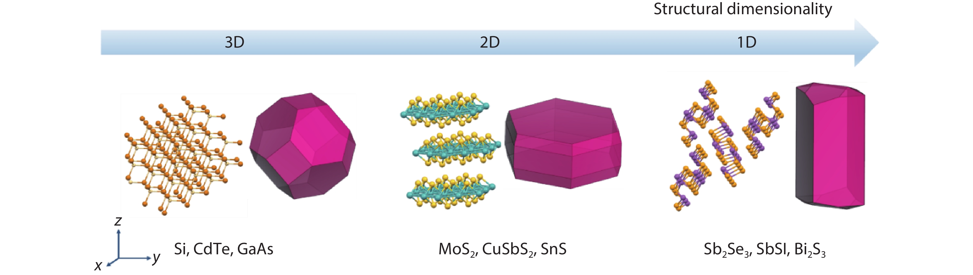
There is a group of compounds with binary and ternary compositions as well as PV-relevant characteristics, which have not been studied extensively because of their reduced structural dimensionality. Low-dimensional materials (namely layered (2D) and chained (1D), see Fig. 1) might be considered to be unsuitable for PV application but have been shown to have potential, both theoretically and experimentally[
![]()
Figure 1.(Color online) The evolution of crystal structure and morphology of the grain as a function of structural dimensionality. CdTe, MoS2 and Sb2Se3 structures were selected as representative materials in each case. Grain morphology was calculated using Bravais−Friedel−Donnay−Harker (BFDH) theory[
There are some excellent reviews on low-dimensional nanomaterials for catalysis, electronics and photonic applications[
Throughout this review we probe material properties that are critical for PV application and correlate them with unique features of low-dimensional materials. In principal, the key condition for good PV material is that diffusion length of photo-generated carriers should be larger than the light penetration depth and can be expressed as
2. Low-dimensional materials for photovoltaic application
2.1. Absorption and band gap
Direct band gap semiconductors are highly favored in many optoelectronic devices and would also be the first prerequisite for an absorber in solar cells. However, providing the difference between direct and indirect gaps, ΔE, is small, semiconductor can be characterized as quasi-indirect type, showing both direct- and indirect-like properties. These characteristics are quite common in low-dimensional materials (Table 1) and, as we will show, are highly suitable for PV devices.
Indirect transition requires the participation of phonon(s) which leads to a lower absorption event probability and therefore low absorption coefficient. However, when the energy of photons is equal or greater than direct gap (Fig. 2(a)), absorption increases abruptly. Therefore, assuming that the ratio of proportional constants between direct and indirect absorption is one tenth, we have calculated the number of photons absorbed in indirect semiconductor with a thickness of 2 μm as a function of ΔE using AM1.5G solar spectrum (dashed line-I in Fig. 2(b), Fig. S1 and Fig. S2). If the indirect band gap of absorber is lower than 1.35 eV, then 85% of photons will be absorbed when ΔE is in the range of 0.125–0.175 eV. For larger band gap absorbers (> 1.35 eV), the conditions are stricter requiring ΔE to be lower than 0.125 eV because of lower photon flux density in the shorter wavelength region of solar spectrum. Evidently, on a theoretical basis, a large part of the solar radiation can still be absorbed by an indirect band gap semiconductor providing that ΔE does not exceed 0.175 eV. Although we have used typical values of absorption parameters (A1 and A2, defined as the proportional constants between absorption coefficient and (hv – Eg)1/2 and (hv – Eg)2, respectively), requirement for ΔE can range (decrease or increase) depending on the material’s absorption capabilities. For instance, for materials with low absorption, ΔE is required to be below 0.1 eV to absorb the same number of photons (Fig. 2(b), dashed line-III, IV).
![]()
Figure 2.(Color online) (a) Photon absorption and carrier dynamics for a quasi-indirect band gap semiconductor. Photons are first absorbed via direct band gap (I) or indirect band gap (II), they then thermodynamically relax to the indirect band gap (III) and eventually recombine (IV). (b) The ratio of photons absorbed to the total number of photons (
2.2. Carrier recombination and lifetime
Besides the light absorption, another key parameter to evaluate the potential of PV material is the carrier lifetime. There is a general consensus that an absorber with > 1 ns of carrier lifetime is necessary to achieve PCE of solar cell over 10% [
When ΔE is in the 0.045–0.175 eV range (for highly absorbing materials) semiconductor can be described as quasi-indirect gap type because of direct-like absorption and indirect-like recombination characteristics. These features are highly desirable in PV materials because they lead to a sufficiently high absorption and long carrier lifetime without sacrificing one or the other. Recently, the quasi-indirect character has been observed in methylammonium lead iodide (CH3NH3PbI3) perovskite (ΔE = 0.04–0.07 eV)[
We acknowledge that quasi-indirect band gap is not a unique feature of low-dimensional materials, but due to low crystal symmetry they possess an indirect type band gap (Table 1). Therefore, materials with low-symmetry structure offer many ways to fully exploit quasi-indirect characteristics, which is highly desirable in PV applications.
2.3. Defects and doping
Understanding the formation of defects and impurities in the semiconductors allows the control of its electrical properties and is important for optimization of functional optoelectronic devices[
![]()
Figure 3.(Color online) Point defects in Sb2Se3 taking into account, it contains two kinds of Sb and three kinds of Se. Reprinted from Chen
2.4. Anisotropy and mobility
Low structural dimensionality leads to the restricted electronic dimensionality and therefore to highly anisotropic carrier movement[
![]()
Figure 4.(Color online) (a) Carrier movement in Sb2Se3 along [120] (red dashed arrows) and [221] (solid red arrow) directions. (b) Atomistic view of Sb2Se3 grain boundary oriented [001] direction perpendicular to substrate. All of the atoms at the edge of these ribbons are saturated (highlighted as red spheres) and introduce no recombination loss at the GBs. Reprinted from Tang
Mobility is one of the parameters describing the transport of photo-generated carriers is the mobility. Assuming zero-optical phonon scattering model carrier mobility depends on effective mass because μ– m*–5/2[
2.5. Surface properties
Another aspect of low-dimensional materials is the large difference in the surface energies of specific facets. This originates from the fact that surfaces terminated by vdW bonds will not produce dangling bonds and will result in low surface energy[
![]()
Figure 5.(Color online) Layered crystal structure of SnS with Pnma space group and calculated morphology of the grain based on the surface energy. Surface energy (SE), EA and IP of various SnS facets. Printed with permission[
2.6. Growth kinetics
The growth principals of low-dimensional materials will differ from 3D because of severe bonding anisotropy. For instance, the classical island growth regime in 3D crystals occurs when atoms are bonded stronger with each other than with substrate, leading to an island-like morphology (Fig. 6(a)). In the case of low-dimensional materials under the same growth conditions, atoms will prefer to bond with each other. However because of large difference in bond strength, adatoms will be preferably attached along the strong bond axis (Fig. 6(b), red arrow). This will lead to the growth of nanowires or sheets parallel to the substrate, which is more characteristic to the layer-by-layer growth regime than the island regime. In 3D materials, a strong interaction of adatoms and substrate atoms will result in layer-by-layer growth regime because the most energetically favored position will be at the terrace forming strong bond with substrate and growing layer (Fig. 6(c)). For low-dimensional materials, a strong interaction with the substrate will lead to nuclei orientation perpendicular to the surface (in terms of strong bond direction), and therefore positions on top of growing nuclei and on substrate will be equally favored leading to growth of nanowires or sheets normal to the substrate (akin to the island-like growth regime), Fig. 6(d). This hypothetical model shows the fundamental difference in growth dynamics of 3D and low-dimensional materials and highlights the importance of the substrate to control film orientation.
![]()
Figure 6.(Color online) Schematics of growth process of 3D and 1D materials on (a, b) inert and (c, d) strongly interacting substrates. (a) represents an island-like growth mode, whereas (c) layer-by-layer[
In thin film solar cells, polycrystalline substrates are commonly employed and therefore will lead to the growth of films with more dispersed orientations than presented above. Commonly, on polycrystalline substrates, the orientation of 3D materials adopts close-packed plane parallel to the surface, i.e. (111) for cubic, (112) for tetragonal or (0001) for hexagonal crystal structures. In contrast, for low-dimensional materials the substrate will play significant role for film orientation, according to the nature of interaction discussed above. For instance, vdW planes in thermally evaporated Bi2S3, Sb2Se3, Sb2S3, SnS and Bi2Se3 films were predominantly oriented parallel to the surface when deposited on inert substrates such as glass or atomically smooth Si[
The properties of the substrate will dictate the orientation of low-dimensional thin films, however, kinetically limited growth conditions can also be used to steer growth dynamics. During the growth of SnS, increased deposition flux reduced the adatom’s surface diffusion length. Consequently instead of thermodynamically favored growth of sparse platelet-like grains, a compact cube-shaped grain morphology was obtained[
2.7. Current research status of solar cells based on low-dimensional materials
Many low-dimensional materials have been explored as potential PV absorbers, such as the one-dimensional Bi2S3, Sb2Se3, Sb2S3 and their alloys, two-dimensional CuSbSe2, CuSbS2, GeSe, SnS, and recently Se and BiOI gained an interest for wide bandgap PV application (Table 1). Among them, the record PCE has been achieved in solar cells with Sb2(Se,S)3 absorber[
3. Conclusion
We discussed and showed that low-dimensional materials could be applied to device level. This broadens the scope of potential application from nanomaterials to the macro-scale devices such as solar cells, photodetectors, light emitting diodes and thermoelectrics. We probed various PV-related material properties and growth mechanism for low-dimensional materials with an aim to provide new insights and design options for functional devices. Low-dimensional materials offer a bright future for various electronic, optic and photonic applications and fabrication of high-quality films with controlled properties will be the next step for their successful implementation.
Acknowledgments
The authors thank the Analytical and Testing Center of HUST and the facility support of the Center for Nanoscale Characterization and Devices (CNCD), WNLO-HUST. This work was supported by the National Natural Science Foundation of China (61725401, 61904058, 61904058), the National Key R&D Program of China (2016YFA0204000), China Postdoctoral Science Foundation Project (2019M662623) and the National Postdoctoral Program for Innovative Talent (BX20190127).
Appendix A. Supplementary materials
Supplementary materials to this article can be found online at https://doi.org/1674-4926/42/3/031701.
References
[1]
[2] M A Green, Y Hishikawa, E D Dunlop et al. Solar cell efficiency tables (version 52). Pro Photovolt, 26, 427(2018).
[3] F Alharbi, J D Bass, A Salhi et al. Abundant non-toxic materials for thin film solar cells: Alternative to conventional materials. Renew Energ, 36, 2753(2011).
[4] J Jean, P R Brown, R L Jaffe et al. Pathways for solar photovoltaics. Energy Environ Sci, 8, 1200(2015).
[5] H Lei, J Chen, Z Tan et al. Review of recent progress in antimony chalcogenide-based solar cells: Materials and devices. Solar RRL, 3, 1900026(2019).
[6] A Mavlonov, T Razykov, F Raziq et al. A review of Sb2Se3 photovoltaic absorber materials and thin-film solar cells. Sol Energy, 201, 227(2020).
[7] L H Wong, A Zakutayev, J D Major et al. Emerging inorganic solar cell efficiency tables (Version 1). J Phys: Energy, 1, 032001(2019).
[8] L Yu, R S Kokenyesi, D A Keszler et al. Inverse design of high absorption thin-film photovoltaic materials. Adv Energy Mater, 3, 43(2013).
[9] L J Phillips, C N Savory, O S Hutter et al. Current enhancement via a TiO2 window layer for CSS Sb2Se3 solar cells: Performance limits and high
[10] Z Li, X Liang, G Li et al. 9.2%-efficient core-shell structured antimony selenide nanorod array solar cells. Nat Commun, 10, 125(2019).
[11] C Liu, L Wang, Y Tang et al. Vertical single or few-layer MoS2 nanosheets rooting into TiO2 nanofibers for highly efficient photocatalytic hydrogen evolution. Appl Catal B, 164, 1(2015).
[12] H J Chuang, B Chamlagain, M Koehler et al. Low-resistance 2D/2D ohmic contacts: A universal approach to high-performance WSe2, MoS2, and MoSe2 transistors. Nano Lett, 16, 1896(2016).
[13] M Zhao, J Su, Y Zhao et al. Sodium-mediated epitaxial growth of 2D ultrathin Sb2Se3 flakes for broadband photodetection. Adv Funct Mater, 30, 1909849(2020).
[14] Z G Chen, X Shi, L D Zhao et al. High-performance SnSe thermoelectric materials: Progress and future challenge. Prog Mater Sci, 97, 283(2018).
[15] T Wu, H Zhang. Piezoelectricity in two-dimensional materials. Angew Chem Int Ed, 54, 4432(2015).
[16] S Niu, G Joe, H Zhao et al. Giant optical anisotropy in a quasi-one-dimensional crystal. Nat Photonics, 12, 392(2018).
[17] H Tian, J Tice, R Fei et al. Low-symmetry two-dimensional materials for electronic and photonic applications. Nano Today, 11, 763(2016).
[18] J D H Donnay, D Harker. A new law of crystal morphology extending the law of Bravais. Am Mineral, 22, 446(1937).
[19] R E Brandt, J R Poindexter, P Gorai et al. Searching for “defect-tolerant” photovoltaic materials: Combined theoretical and experimental screening. Chem Mater, 29, 4667(2017).
[20] A Othonos. Probing ultrafast carrier and phonon dynamics in semiconductors. J App Phys, 83, 1789(1998).
[21] E M Hutter, M C Gélvez-Rueda, A Osherov et al. Direct–indirect character of the bandgap in methylammonium lead iodide perovskite. Nat Mater, 16, 115(2016).
[22] M Saliba, J P Correa-Baena, C M Wolff et al. How to make over 20% efficient perovskite solar cells in regular (n–i–p) and inverted (p–i–n) architectures. Chem Mater, 30, 4193(2018).
[23] A Walsh, A Zunger. Instilling defect tolerance in new compounds. Nat Mater, 16, 964(2017).
[24] J Vidal, S Lany, M d’Avezac et al. Band-structure, optical properties, and defect physics of the photovoltaic semiconductor SnS. Appl Phys Lett, 100, 032104(2012).
[25] Y Huang, C Wang, X Chen et al. First-principles study on intrinsic defects of SnSe. RSC Advances, 7, 27612(2017).
[26] D Han, M H Du, C M Dai et al. Influence of defects and dopants on the photovoltaic performance of Bi2S3: first-principles insights. J Mater Chem A, 5, 6200(2017).
[27] M Huang, P Xu, D Han et al. Complicated and unconventional defect properties of the quasi-one-dimensional photovoltaic semiconductor Sb2Se3. ACS Appl Mater Inter, 11, 15564(2019).
[28] J Qiao, X Kong, Z X Hu et al. High-mobility transport anisotropy and linear dichroism in few-layer black phosphorus. Nat Commun, 5, 4475(2014).
[29] Y Zhou, L Wang, S Chen et al. Thin-film Sb2Se3 photovoltaics with oriented one-dimensional ribbons and benign grain boundaries. Nat Photonics, 9, 409(2015).
[30] K S Novoselov, A Mishchenko, A Carvalho et al. 2D materials and van der Waals heterostructures. Science, 353, aac9439(2016).
[31] A W Welch, L L Baranowski, P Zawadzki et al. Accelerated development of CuSbS2 thin film photovoltaic device prototypes. Pro Photovoltaics, 24, 929(2016).
[32] T Kirchartz, U Rau. What makes a good solar cell. Adv Energy Mater, 8, 1703385(2018).
[33] L R Gilbert, B Van Pelt, C Wood. The thermal activation energy of crystalline Sb2Se3. J Phys Chem Solids, 35, 1629(1974).
[34] Y Chen, Y Sun, J Peng et al. Tailoring organic cation of 2D air-Stable organometal halide perovskites for highly efficient planar solar cells. Adv Energy Mater, 7, 1700162(2017).
[35] H Tsai, W Nie, J C Blancon et al. High-efficiency two-dimensional Ruddlesden–Popper perovskite solar cells. Nature, 536, 312(2016).
[36] M M Nassary. Temperature dependence of the electrical conductivity, Hall effect and thermoelectric power of SnS single crystals. J Alloy Compd, 398, 21(2005).
[37] P Sinsermsuksakul, L Sun, S W Lee et al. Overcoming efficiency limitations of SnS-based solar cells. Adv Energy Mater, 4, 1400496(2014).
[38] L D Zhao, G Tan, S Hao et al. Ultrahigh power factor and thermoelectric performance in hole-doped single-crystal SnSe. Science, 351, 141(2016).
[39] A W Welch, L L Baranowski, H Peng et al. Trade-offs in thin film solar cells with layered chalcostibitephotovoltaic absorbers. Adv Energy Mater, 7, 1601935(2017).
[40] K Ramasamy, H Sims, W H Butler et al. Mono-, few-, and multiple layers of copper antimony sulfide (CuSbS2): A ternary layered sulfide. J Am Chem Soc, 136, 1587(2014).
[41] S Banu, S J Ahn, S K Ahn et al. Fabrication and characterization of cost-efficient CuSbS2 thin film solar cells using hybrid inks. Sol Energ Mat Sol C, 151, 14(2016).
[42] W Kautek. Electronic mobility anisotropy of layered semiconductors: transversal photoconductivity measurements at n-MoSe2. J Phys C, 15, L519(1982).
[43] Z Chen, H Liu, X Chen et al. Wafer-size and single-crystal MoSe2 atomically thin films grown on GaN substrate for light emission and harvesting. ACS Appl Mater Inter, 8, 20267(2016).
[44] B Evans, P Young. Optical absorption and dispersion in molybdenum disulphide. Proc R Soc London Ser A, 284, 402(1965).
[45] S Wi, H Kim, M Chen et al. Enhancement of photovoltaic response in multilayer MoS2 induced by plasma doping. ACS Nano, 8, 5270(2014).
[46] D S Kyriakos, A N Anagnostopoulos. Electrical conductivity of layered GeSe related to extended faults. J App Phys, 58, 3917(1985).
[47] D J Xue, S C Liu, C M Dai et al. GeSe thin-film solar cells fabricated by self-regulated rapid thermal sublimation. J Am Chem Soc, 139, 958(2017).
[48] B R Chakraborty, B Ray, R Bhattacharya et al. Magnetic and electric properties of antimony selenide (Sb2Se3) crystals. J Phys Chem Solids, 41, 913(1980).
[49] B Roy, B R Chakraborty, R Bhattacharya et al. Electrical and magnetic properties of antimony sulphide (Sb2S3) crystals and the mechanism of carrier transport in it. Solid State Commun, 25, 937(1978).
[50] Y C Choi, D U Lee, J H Noh et al. Highly improved Sb2S3 sensitized-inorganic–organic heterojunction solar cells and quantification of traps by deep-level transient spectroscopy. Adv Function Mater, 24, 3587(2014).
[51] X Wang, R Tang, C Jiang et al. Manipulating the electrical properties of Sb2(S,Se)3 film for high-efficiency solar cell. Adv Energy Mater, 10, 2002341(2020).
[52] A Cantarero, J Martinez-Pastor, A Segura et al. Transport properties of bismuth sulfide single crystals. Phys Rev B, 35, 9586(1987).
[53] H Song, X Zhan, D Li et al. Rapid thermal evaporation of Bi2S3 layer for thin film photovoltaics. Sol Energ Mat Sol C, 146, 1(2016).
[54] M Yoshida, K Yamanaka, Y Hamakawa. Semiconducting and dielectric properties of c-axia oriented SbSI thin film. Jpn J Appl Phys, 12, 1699(1973).
[55] R Nie, H S Yun, M J Paik et al. Efficient solar cells based on light-harvesting antimony sulfoiodide. Adv Energy Mater, 8, 1701901(2018).
[56] R L Z Hoye, L C Lee, R C Kurchin et al. Strongly enhanced photovoltaic performance and defect physics of air-stable bismuth oxyiodide (BiOI). Adv Mater, 29, 1702176(2017).
[57] T K Todorov, S Singh, D M Bishop et al. Ultrathin high band gap solar cells with improved efficiencies from the world's oldest photovoltaic material. Nat Commun, 8, 682(2017).
[58] A Koma. New epitaxial growth method for modulated structures using van der Waals interactions. Surf Sci, 267, 29(1992).
[59] B Yang, C Wang, Z Yuan et al. Hydrazine solution processed CuSbSe2: Temperature dependent phase and crystal orientation evolution. Sol Energ Mat Sol C, 168, 112(2017).
[60] R Jaccodine. Surface energy of germanium and silicon. J Electrochem Soc, 110, 524(1963).
[61] V Stevanović, K Hartman, R Jaramillo et al. Variations of ionization potential and electron affinity as a function of surface orientation: The case of orthorhombic SnS. Appl Phys Lett, 104, 211603(2014).
[62]
[63] M E Rincón, M Sánchez, P J George et al. Comparison of the properties of bismuth sulfide thin films prepared by thermal evaporation and chemical bath deposition. J Solid State Chem, 136, 167(1998).
[64] T M Razykov, A X Shukurov, O K Atabayev et al. Growth and characterization of Sb2Se3 thin films for solar cells. Sol Energy, 173, 225(2018).
[65] Y S Mayon, T P White, R Wang et al. Evaporated and solution deposited planar Sb2S3 solar cells: A comparison and its significance. Phys Status Solid A, 213, 108(2016).
[66] P A Nwofe, K T R Reddy, G Sreedevi et al. Single phase, large grain, p-conductivity-type SnS layers produced using the thermal evaporation method. Energy Procedia, 15, 354(2012).
[67] M Zhang, L Lv, Z Wei et al. Thermal evaporation growth of topological insulator Bi2Se3 thin films. Mater Lett, 123, 87(2014).
[68] N Solayappan, K K Raina, R K Pandey et al. Role of antimony sulfide buffer layers in the growth of ferroelectric antimony sulfo-iodide thin films. J Mater Res, 12, 825(1997).
[69] J Varghese, C O’Regan, N Deepak et al. Surface roughness assisted growth of vertically oriented ferroelectric SbSI nanorods. Chem Mater, 24, 3279(2012).
[70] R Kondrotas, J Zhang, C Wang et al. Growth mechanism of Sb2Se3 thin films for photovoltaic application by vapor transport deposition. Sol Energ Mat Sol C, 199, 16(2019).
[71] A Mavlonov, A Shukurov, F Raziq et al. Structural and morphological properties of PLD Sb2Se3 thin films for use in solar cells. Sol Energy, 208, 451(2020).
[72] D Lim, H Suh, M Suryawanshi et al. Kinetically controlled growth of phase-pure SnS absorbers for thin film solar cells: Achieving efficiency near 3% with long-term stability using an SnS/CdS heterojunction. Adv Energy Mater, 8, 1702605(2018).
[73] C Chen, J Tang. Open-crcuit voltage loss of antimony chalcogenide solar cells: status, origin, and possible solutions. ACS Energy Lett, 5, 2294(2020).
[74] G X Liang, Y D Luo, S Chen et al. Sputtered and selenized Sb2Se3 thin-film solar cells with open-circuit voltage exceeding 500 mV. Nano Energy, 73, 104806(2020).
[75] T D C Hobson, L J Phillips, O S Hutter et al. Isotype heterojunction solar cells using n-type Sb2Se3 thin films. Chem Mater, 32, 2621(2020).


Set citation alerts for the article
Please enter your email address

© Copyright 2018-2021 | Chinese Laser Press. All Rights Reserved 沪ICP备15018463号-20