• Photonics Research
  • Vol. 7, Issue 7, 815 (2019)
Huan Jiang1、2, Sajid Choudhury2, Zhaxylyk A. Kudyshev2, Di Wang2, Ludmila J. Prokopeva2, Peng Xiao3, Yongyuan Jiang1、4、5、6、7, and Alexander V. Kildishev2、*
Author Affiliations
  • 1Institute of Modern Optics, Department of Physics, Harbin Institute of Technology, Harbin 150001, China
  • 2School of Electrical and Computer Engineering and Birck Nanotechnology Center, Purdue University, West Lafayette, Indiana 47907, USA
  • 3School of Electrical Engineering and Automation, Harbin Institute of Technology, Harbin 150001, China
  • 4Collaborative Innovation Center of Extreme Optics, Shanxi University, Taiyuan 030006, China
  • 5Key Laboratory of Micro-Optics and Photonic Technology of Heilongjiang Province, Harbin 150001, China
  • 6Key Laboratory of Micro-Nano Optoelectronic Information System of Ministry of Industry and Information Technology, Harbin 150001, China
  • 7e-mail: jiangyy@hit.edu.cn
  • show less
    DOI: 10.1364/PRJ.7.000815 Cite this Article Set citation alerts
    Huan Jiang, Sajid Choudhury, Zhaxylyk A. Kudyshev, Di Wang, Ludmila J. Prokopeva, Peng Xiao, Yongyuan Jiang, Alexander V. Kildishev. Enhancing sensitivity to ambient refractive index with tunable few-layer graphene/hBN nanoribbons[J]. Photonics Research, 2019, 7(7): 815 Copy Citation Text show less
    Schematics of the proposed device. (a) The G3BN2 ribbon array on top of dielectric ribbons is separated from the Au substrate by a dielectric spacer (t1=30 nm and t2=322 nm). (b) The cross-sectional view of the sensor in the x–z-plane, with a period p=160 nm and width w=80 nm.
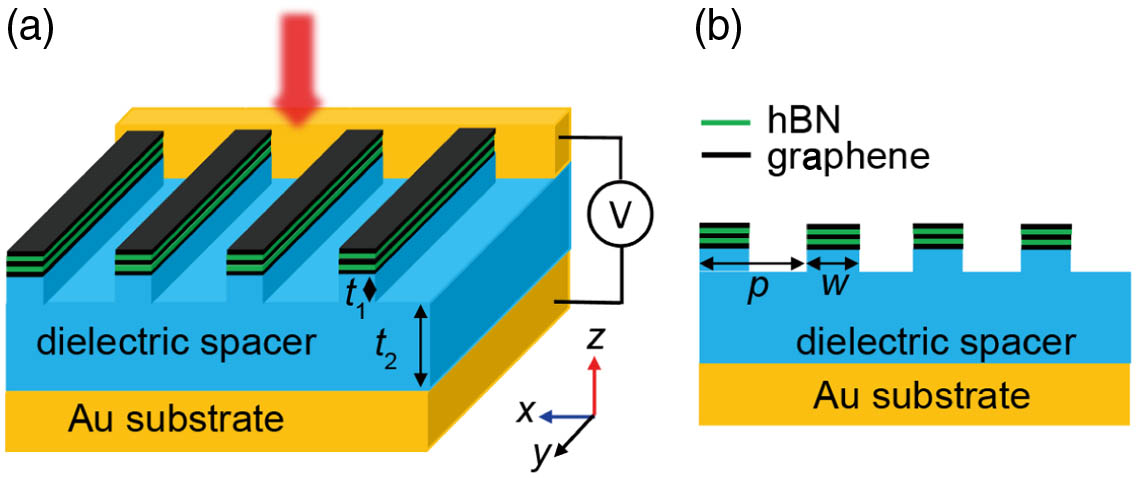
    Fig. 1. Schematics of the proposed device. (a) The G3BN2 ribbon array on top of dielectric ribbons is separated from the Au substrate by a dielectric spacer (t1=30  nm and t2=322  nm). (b) The cross-sectional view of the sensor in the xz-plane, with a period p=160  nm and width w=80  nm.
    G3BN2 few-layer ribbon array with a higher Q and an MD larger than those of G1BN1 and G2BN1. (a) Reflectance spectra of the G1BN1, G2BN1, and G3BN2 ribbon arrays excited by incident light with the electric field perpendicular to graphene ribbon. (b) Reflectance spectra with different charge scattering times. The color map of the E-field magnitude distribution in the vicinity of (c) G1BN1, (d) G2BN1, and (e) G3BN2 ribbons in the x–z-plane at the resonant wavelengths of 10.857, 8.068, and 6.786 μm, respectively.
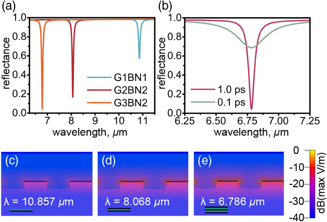
    Fig. 2. G3BN2 few-layer ribbon array with a higher Q and an MD larger than those of G1BN1 and G2BN1. (a) Reflectance spectra of the G1BN1, G2BN1, and G3BN2 ribbon arrays excited by incident light with the electric field perpendicular to graphene ribbon. (b) Reflectance spectra with different charge scattering times. The color map of the E-field magnitude distribution in the vicinity of (c) G1BN1, (d) G2BN1, and (e) G3BN2 ribbons in the xz-plane at the resonant wavelengths of 10.857, 8.068, and 6.786 μm, respectively.
    Sensing process of the proposed sensor. (a) The cross-sectional view of the proposed sensor with the analyte; the thickness of the analyte above graphene is ta. (b) Reflectance spectra of different analytes with different RIs (n=1.50–1.52).
    Fig. 3. Sensing process of the proposed sensor. (a) The cross-sectional view of the proposed sensor with the analyte; the thickness of the analyte above graphene is ta. (b) Reflectance spectra of different analytes with different RIs (n=1.501.52).
    Dependence of the resonance position on the RIs of analytes. (a) The reflectance spectra of the proposed sensor for 100-nm-thick analytes with different RIs n=1.00–2.00 (EF=0.25 eV), (b) the resonant spectral position for different RI analytes, (c) sensitivity (m) and FWHM, and (d) FOM and quality factors (Q) as a function of analytes’ RIs.
    Fig. 4. Dependence of the resonance position on the RIs of analytes. (a) The reflectance spectra of the proposed sensor for 100-nm-thick analytes with different RIs n=1.002.00 (EF=0.25  eV), (b) the resonant spectral position for different RI analytes, (c) sensitivity (m) and FWHM, and (d) FOM and quality factors (Q) as a function of analytes’ RIs.
    A precondition for accurate sensing is to keep the analyte thickness above 60 nm. (a) The resonant wavelengths with different thicknesses of analytes from 1 to 200 nm (EF=0.25 eV). (b) Working bands of the reflectance sensor can be selected by controlling graphene’s Fermi energy (n=1.75).
    Fig. 5. A precondition for accurate sensing is to keep the analyte thickness above 60 nm. (a) The resonant wavelengths with different thicknesses of analytes from 1 to 200 nm (EF=0.25  eV). (b) Working bands of the reflectance sensor can be selected by controlling graphene’s Fermi energy (n=1.75).
    Polarization-dependent reflectance of the G3BN2 sensor (n=1.00).
    Fig. 6. Polarization-dependent reflectance of the G3BN2 sensor (n=1.00).
    Dielectric function of CaF2 [43].
    Fig. 7. Dielectric function of CaF2 [43].
    Surface conductivity of graphene calculated using the RPA model for room temperature T=300 K, Fermi energies EF=0.25 and 0.3 eV, and relaxation time τ obtained from Eq. (2) in the main text. The pink area indicates the wavelength range of interest (6–11 μm). (a) Real and (b) imaginary parts of total relative conductivity; (c) absolute error between two formulations, Eqs. (C1) and (C2); and (d) intraband and (e) interband responses calculated for EF=0.3 eV.
    Fig. 8. Surface conductivity of graphene calculated using the RPA model for room temperature T=300  K, Fermi energies EF=0.25 and 0.3 eV, and relaxation time τ obtained from Eq. (2) in the main text. The pink area indicates the wavelength range of interest (6–11 μm). (a) Real and (b) imaginary parts of total relative conductivity; (c) absolute error between two formulations, Eqs. (C1) and (C2); and (d) intraband and (e) interband responses calculated for EF=0.3  eV.
    Components of the hBN dielectric function [48] (a) in-plane and (b) out-of-plane.
    Fig. 9. Components of the hBN dielectric function [48] (a) in-plane and (b) out-of-plane.
    Reflectance spectra of (a) G1BN1, (b) G2BN2, and (c) G3BN2 ribbon arrays with different analytes (n=1.00 and n=2.00).
    Fig. 10. Reflectance spectra of (a) G1BN1, (b) G2BN2, and (c) G3BN2 ribbon arrays with different analytes (n=1.00 and n=2.00).
    Published RI Sensors (year published)Wavelength (μm)Max Sensitivity (μm/RIU)Max FOMQuality Factor
    T-shaped crystal waveguide (2017) [10]2.41.04//
    Metal–insulator–metal waveguides (2015) [14]21.57//
    Slotted photonic crystal waveguides (2017) [15]3.61.15//
    Fiber-optic couplers (2017) [20]1.52.17//
    Graphene disk-gold ring (2015) [1]11.5 THz (26  μm)2.8 (1.9 THz/RIU)6.559
    Graphene on dielectric grating (2017) [36]7.32.510.7/
    Ag-graphene hybrid grating structure (2016) [37]2.8/20/
    G3BN2 ribbon sensor in this paper6.8, 10.33.1, 4.257.5, 27.1125.6, 66.7
    Table 1. Comparison with the Published Sensors
    Huan Jiang, Sajid Choudhury, Zhaxylyk A. Kudyshev, Di Wang, Ludmila J. Prokopeva, Peng Xiao, Yongyuan Jiang, Alexander V. Kildishev. Enhancing sensitivity to ambient refractive index with tunable few-layer graphene/hBN nanoribbons[J]. Photonics Research, 2019, 7(7): 815
    Download Citation