Huan Jiang1、2, Sajid Choudhury2, Zhaxylyk A. Kudyshev2, Di Wang2, Ludmila J. Prokopeva2, Peng Xiao3, Yongyuan Jiang1、4、5、6、7, and Alexander V. Kildishev2、*
Huan Jiang, Sajid Choudhury, Zhaxylyk A. Kudyshev, Di Wang, Ludmila J. Prokopeva, Peng Xiao, Yongyuan Jiang, Alexander V. Kildishev. Enhancing sensitivity to ambient refractive index with tunable few-layer graphene/hBN nanoribbons[J]. Photonics Research, 2019, 7(7): 815
Copy Citation Text
Refractive index (RI) sensing helps to identify biomolecules and chemicals in the mid-infrared range for drug discovery, bioengineering, and environmental monitoring. In this paper, we numerically demonstrate an electrically tunable RI sensor with ultrahigh sensitivity using a three-layer graphene nanoribbon array separated by hexagonal boron nitride (hBN). Unlike the weak resonance in single-layer graphene nanoribbons, a much stronger plasmon resonance featuring a higher-quality factor can be excited in the graphene/hBN few-layer ribbon array. Simultaneously, the high purity of graphene on hBN results in an outstanding charge mobility above at 300 K, which allows a larger modulation depth. The interaction between the locally enhanced field around graphene ribbons and its surrounding analyte leads to ultrahigh sensitivity (4.207 μm/RIU), with the figure of merit reaching approximately 58. Moreover, this ultrasensitive detector could selectively work in different wavebands by controlling gate voltages applied to graphene. These merits of ultrahigh sensitivity and electrical tunability are major advances compared to previous RI sensors, paving a way toward ultrasensitive detection using graphene/hBN few-layer devices.
1. INTRODUCTION
Refractive index (RI, ) sensing is of great scientific and technological interest, especially in the mid-infrared (mid-IR) range because of its broad use in identifying biological and chemical agents. Different agents such as air-dried Herring DNA () and ovalbumin (), polytetrafluoroethylene (PTFE) (), trinitrotoluene (TNT) (), cyclotrimethylenetrinitramine (RDX) (), and cyclotetramethylenete-tranitramine (HMX) () have been identified using RI sensing [1–3]. Generally, sensors based on optical sensing mechanisms exhibit a stronger response to RI change with the variation of spectra [4], phase [5], and amplitude [6] than magnetic field- [7], mechanical force- [8], and temperature-based [9] sensors. Typically, the sensing mechanism in spectral sensing relies on the rate of resonant wavelength shift with respect to the change in the RI, where the main metrics are sensitivity, modulation depth, and quality factor. Equations and define the sensitivity () [10] and quality factor (), respectively, where is the resonant wavelength, and FWHM is the full width at half maximum of the resonance peak. The ratio defines the modulation depth (MD), where and denote the maximum and minimum values in the reflectance spectra, respectively. To obtain high sensitivity, a high- resonance mode is desirable, as a sharp extremum facilitates an easier detection of the resonant wavelength shift caused by a subtle RI variation of the surrounding medium. In recent years, various types of meta-material sensors have been developed, which rely on T-shaped slots [10], nanowires [11], fibers [12,13], plasmonic waveguides [14–16], the Fabry–Perot cavity [17,18], Fano resonance structures [1,19–22], and other designs [23–30]. Despite the good sensing performance enabled by recent developments in photonic technologies, the static sensors’ lack of active tunability limits both their working wavebands and the analyte categories. In pursuit of dynamic sensing devices, a frequency-tunable RI sensor with a mechanically stretchable substrate has been reported [31], but slow tuning speed and complex configuration still restrict its applications.
Graphene, a two-dimensional layer of carbon atoms arranged in a honeycomb lattice, not only supports surface plasmons with higher confinement and lower loss than metals do, but its electrical/optical properties can also be effectively tuned by electrical gating. Graphene’s Fermi energy can be rapidly changed via gate voltage in the field-effect transistor (FET) structures; this feature makes graphene a promising material in configurable devices in the IR and terahertz (THz) regions [32,33]. To date, several tunable RI sensors using monolayer graphene [34,35] or its hybrid structures have been reported [1,36–38]. These sensors use the shift of the graphene plasmon resonant wavelength as a tool to detect small changes in the ambient RI in the vicinity of the graphene-based structure. Although significant progress has been made in enhancing the sensing speed and optimizing the structure of graphene tunable sensors, there are still fundamental roadblocks to enhancing their sensing performance due to the relatively weak plasmon resonance in monolayer graphene. It has been observed that the charge mobility of graphene strongly depends on the quality of graphene. The combination of graphene and hexagonal boron nitride (hBN) can significantly improve the purity of graphene due to their lattice matching [39,40], so the graphene in contact with hBN has superior electrical/optical properties. Here, we propose two methods to obtain high- resonance with a large MD: one through cascading graphene layers, and the other via improving the purity of graphene, i.e., by combining graphene with hBN. We then show that we can achieve an ultrasensitive RI sensor by patterning graphene/hBN few-layer structure into a ribbon array. Our paper is organized as follows. Section 2 discusses the numerical simulations and design of the RI sensor and how the various materials are modeled in our design approach. Section 3 shows the sensitivity and FOM of the proposed sensor and compares them to previously published RI sensors. Finally, Section 4 summarizes the results of our study and provides a future outlook.
2. DESIGN AND NUMERICAL SIMULATIONS
To improve the sensing performance of an RI sensor, one needs to excite high- resonance with large MD, which is possible to achieve by exciting plasmon resonance in a graphene nanoribbon array. In an appropriately designed graphene nanoribbon structure, propagating electromagnetic waves can be directly coupled to the bounded collective charge oscillations in graphene, giving rise to plasmon resonance [41]. We utilize an elaborate graphene/hBN nanoribbon array with high graphene purity to enhance the plasmon resonance. What’s more, increasing the number of graphene/hBN ribbon layers further enhances the plasmon resonance, leading to a higher- device [42]. Considering the ease of fabrication, we choose the G3BN2 nanoribbon array (hereinafter, we use the notation , with and being the number of graphene and hBN ribbon layers, respectively).
Sign up for Photonics Research TOC. Get the latest issue of Photonics Research delivered right to you!Sign up now
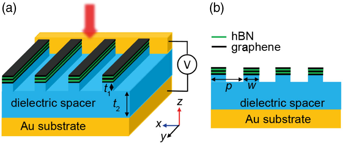
As shown in Fig. 1(a), the graphene/hBN few-layer ribbon array on the top of ribbons is placed on a gold substrate separated by a dielectric spacer. The layer marked in the black color represents single-layer graphene, and the layer marked in the green color represents 1-nm-thick hBN, which is about two atomic layers. is chosen as the spacer material because its permittivity in the mid-IR has smaller dispersion compared to other dielectric materials, e.g., or . In the waveband from 6.786 to 10.431 μm, the proposed structure is optimized with the following geometry: an array period of , a width of for both G3BN2 and ribbons, a ribbon thickness , and a spacer thickness , respectively. The ribbon is designed to account for possible tolerance to over-etching. In our simulation model, a normally incident linearly polarized light, with its -field polarized perpendicularly to the ribbons (in the -direction), is used to illuminate the structure. Note that the incident light with its -field polarized parallelly to the ribbons (in the -direction), which is completely reflected by the structure (see Appendix A), cannot excite the plasmon resonance. The reflectance spectrum is simulated using a commercial solver based on the finite element method in the frequency domain (CST Studio). The boundary conditions are periodic in - and -directions (transverse to light propagation direction) and open for -directions in free space.
Figure 1.Schematics of the proposed device. (a) The G3BN2 ribbon array on top of dielectric ribbons is separated from the Au substrate by a dielectric spacer ( and ). (b) The cross-sectional view of the sensor in the -plane, with a period and width .
The dielectric functions of and Au are taken from the experiment [43] (see Appendix B) and Ref. [44], respectively. For reduced computational cost and improved simulation robustness, graphene is modeled using surface impedance [41], where the surface conductivity of graphene is calculated using a new integration-free formulation [45] for the random phase approximation (RPA) model [46,47]: Here is digamma function, and the fundamental constants, , , , and are the electron charge, the Boltzmann constant, the reduced Planck constant, and the universal conductivity, respectively. The temperature and Fermi energy are renormalized to rad/s units using notations and . (For comparison with classical RPA formulation, see Appendix C.) The relaxation time and charge mobility are related by [48,49] where the DC mobility of graphene on the hBN substrate is at 300 K [39,50], is the Fermi velocity, and the Fermi energy typically ranges from 0.25 to 0.3 eV [41]. According to Eq. (1), graphene’s conductivity depends on angular frequency , temperature , Fermi energy , and relaxation time . The hBN permittivity is taken from Refs. [48,51,52] (see Appendix D).
We compare the sensitivity of the G3BN2 ribbon array versus the sensitivity of the G1BN1 and G2BN2 ribbon arrays. The wavelength shift of the G3BN2 ribbon array, caused by the same refractive index change, is the largest (see Appendix E). But sensitivity does not solely define the capability to detect and quantify the refractive indexes of analytes. The sensor resolution characterized by the smallest discernible spectral shift is equally important. In turn, the sensor resolution is closely related to MD and FWHM; for example, if the wavelength shifts larger than FWHM/2 then any two spectral peaks are robustly discernible. The reflectance spectra of the G1BN1, G2BN2, and G3BN2 ribbon arrays with the graphene Fermi energy of 0.25 eV are calculated. In Fig. 2(a), the spectrum of the G3BN2 ribbon array exhibits stronger resonances with larger MD than the ones of G1BN1 and G2BN1 ribbon arrays. The MD of G3BN2 ribbon array (0.98) is significantly enhanced compared to the MDs of G1BN1 (0.54) and G2BN1 (0.78) ribbon arrays. Meanwhile, the reflectance linewidth of G3BN2 ribbon array characterized by FWHM value (54 nm) is also the narrowest. The larger MD and narrower linewidth result from the much stronger plasmon resonance in the G3BN2 ribbon array, as the multiple layers have additional free charges as compared to single-layer graphene. Therefore, accumulating the number of the graphene layers results in a larger equivalent conductivity, which leads to a high- plasmon resonance. The -field distributions in the -plane in Figs. 2(c)–2(e) illustrate the stronger field confinement of the G3BN2 compared to the G1BN1 and G2BN1 ribbon arrays at their resonant wavelengths.
Figure 2.G3BN2 few-layer ribbon array with a higher and an MD larger than those of G1BN1 and G2BN1. (a) Reflectance spectra of the G1BN1, G2BN1, and G3BN2 ribbon arrays excited by incident light with the electric field perpendicular to graphene ribbon. (b) Reflectance spectra with different charge scattering times. The color map of the -field magnitude distribution in the vicinity of (c) G1BN1, (d) G2BN1, and (e) G3BN2 ribbons in the -plane at the resonant wavelengths of 10.857, 8.068, and 6.786 μm, respectively.
The use of graphene combined with hBN further enhances the plasmon resonance in the G3BN2 ribbon array. The measured mobility of graphene on the hBN substrate ranges from to at 300 K in Ref. [39]. We take the mobility of [corresponding to a scattering time according to Eq. (2)]. For comparison, we also use a mobility of (), consistent with the reported mobility of graphene on substrate [between and ] [39,40,50]. Figure 2(b) shows reflectance spectra of the G3BN2 ribbon array with 0.25 eV Fermi energy at different scattering times corresponding to graphene on hBN () and graphene on (). It is evident that G3BN2 with 1 ps scattering time for graphene has a higher with a higher MD and smaller FWHM than the one with 0.1 ps. Hence, the use of graphene combined with hBN further enhances the resolution of the proposed sensor, and therefore multilayer graphene/hBN RI sensors have the potential to outperform single-layered RI sensors.
3. RESULTS AND DISCUSSION
Within our system, one can measure the analytes’ RIs through detecting the reflectance spectra of the targeted analytes surrounding graphene/hBN ribbons. Figure 3(a) shows the cross-sectional view of the proposed G3BN2 ribbon array with an analyte. The analyte layer on the top of graphene has a thickness . To measure the wavelength shift caused by a slight RI variation, we calculate reflectance spectra under normal incidence using for different analytes with RIs ranging from 1.50 to 1.52 in steps of 0.01 [Fig. 3(b)]. Even a moderate RI change of causes a 73 nm wavelength shift from 8.415 to 8.488 μm. Also, an average FWHM of reflectance spectra for RIs changing from 1.50 to 1.52 is approximately 103 nm [Fig. 3(b)]. The small FWHM enables one to measure the minute spectral shift caused by slight RI change, increasing the resolution of the proposed sensor.
Figure 3.Sensing process of the proposed sensor. (a) The cross-sectional view of the proposed sensor with the analyte; the thickness of the analyte above graphene is . (b) Reflectance spectra of different analytes with different RIs ().
The proposed G3BN2 sensor can detect a large category of analytes. We show the reflectance spectra with RIs from 1.00 to 2.00 in steps of 0.25 as shown in Fig. 4(a). The sharp reflectance dips shift from 6.786 to 10.431 μm as the analyte’s RI increases from 1.00 to 2.00. To quantitatively evaluate the sensitivity of the proposed sensor, Fig. 4(b) shows the spectral positions with the variation of analyte’s RIs and its quadratic fitting as . The resonant wavelength of the sensor system nonlinearly shifts to longer wavelength as RI increases, which causes the sensitivity to be RI dependent. The sensitivity increases from 3.104 μm/RIU to 4.207 μm/RIU when the RI increases from 1.00 to 2.00 [see Fig. 4(c)]. The confined -field resulting from plasmon resonance close to graphene ribbons in Fig. 2(e) is strongly affected by analyte’s RI. As expected, the larger the RI of a given analyte, the stronger wavelength shift. Also, the FWHM increases from 54 to 155 nm with the increase of RI from 1.00 to 2.00 [as shown in Fig. 4(c)]. The FOM, defined as [53], is up to 57.47 in the detection region, as shown in Fig. 4(d). We also present the values of for different RI analytes () in Fig. 4(d). The maximum of reflectance reaches 125.61 at .
Figure 4.Dependence of the resonance position on the RIs of analytes. (a) The reflectance spectra of the proposed sensor for 100-nm-thick analytes with different RIs (), (b) the resonant spectral position for different RI analytes, (c) sensitivity () and FWHM, and (d) FOM and quality factors () as a function of analytes’ RIs.
Except for analyte’s RI, the resonant wavelength is also affected by analyte’s volume and graphene’s Fermi energy. To avoid the sensing error induced by analyte’s thickness, we investigate the relationship between the resonant wavelength and the thickness of analytes . The resonant wavelength for analytes with red shifts when the analyte thickness increases from 0 to 60 nm, while it remains unchanged when the analyte thickness is greater than 60 nm [Fig. 5(a)]. The analyte thickness () does not depend on the resonant wavelength because -fields are mainly localized within the 60 nm layer close to graphene surface. Thus, to avoid the spectral shift caused by analyte thickness, we need at least 60-nm-thick analyte films.
Figure 5.A precondition for accurate sensing is to keep the analyte thickness above 60 nm. (a) The resonant wavelengths with different thicknesses of analytes from 1 to 200 nm (). (b) Working bands of the reflectance sensor can be selected by controlling graphene’s Fermi energy ().
Some specific biological or chemical molecules have intrinsic absorption in the IR band, e.g., the carbonyl double-bond () [54]. The waveband of our sensor can be tuned to avoid such intrinsic absorptions, thus improving the overall ability to sense analytes’ RIs. The Fermi energy of graphene can be tuned by applying a gate voltage in an FET structure, resulting in the tunability of working waveband. The Fermi energy level of graphene can be tuned with applied electric field realistically from 0.20 eV to 0.40 eV. As expected, with the Fermi energy of graphene varying from 0.20 to 0.40 eV, the reflectance dip for the analyte with blue shifts 3.192 μm from 10.517 to 7.325 μm, as depicted in Fig. 5(b), which is consistent with the Drude-like model. Thus, one can accurately identify the RI of analytes from 1.00 to 2.00 using the sensor in the desired waveband via electric gating.
Table 1 compares the sensing performance of the proposed G3BN2 sensor with some of the recently published studies. The first four sensors in Table 1 utilize waveguides and fiber-optic couplers with fixed working wavebands. However, the next three sensors employ graphene with electrically tunable working wavebands. The parameters in the last row are listed for the G3BN2 ribbon array sensor suggested in this paper. Our sensor shows superior metrics regarding sensitivity, FOM, and compared with recently reported sensors. To summarize, this section deals with the different sensing performance metrics of previously published sensors and compares our RI sensor with them, which shows that our optimized G3BN2 ribbon sensor exhibits a highly competitive sensing performance.
We designed and optimized an electrically tunable RI sensor consisting of a graphene/hBN few-layer ribbon array for operation in the mid-IR region. The design optimization of the device employed the interband part of the graphene surface conductivity approximated with a fast integration-free version of the Kubo formula rewritten as a difference of digamma functions. The optimized RI sensor exhibits a high sensitivity (4.207 μm/RIU) and a large FOM (57.47) in comparison to published sensors. The sensor can identify RIs of analytes () using the shift of resonant wavelength when the thickness of the analyte is thicker than 60 nm. Furthermore, the highly sensitive device can selectively operate within desired wavebands through electrically tuning the Fermi energy of graphene ribbons. The largely enhanced sensitivity and the tunable selectivity of the working waveband are the major advances of our sensor. Furthermore, higher sensitivity can be achieved by designing the Fabry–Perot cavity with our few-layer graphene sensor, as such a cavity has been demonstrated to have a higher FOM [17,18]. The highly sensitive sensor shows excellent promise for potential applications in sensing chemicals and biomolecules in the mid-IR region.
APPENDIX A: POLARIZATION-DEPENDENT REFLECTANCE
We calculate the reflectance spectra for the incident light with the electric field parallel and perpendicular to the ribbons. The incident light polarized parallelly to the ribbons (-polarized) cannot excite the plasmon resonance, so there is no reflectance dip, and the magnitude of reflectance is close to one. But the light polarized perpendicularly to the ribbons (-polarized) excites strong plasmon resonance, so there is a sharp dip in the reflectance spectra, as shown in Fig. 6.
Figure 6.Polarization-dependent reflectance of the G3BN2 sensor ().
The approximated experimental data of the dielectric function are shown in Fig. 7. The dispersion formula of is obtained from the empirical Sellmeier approximation [43]: where is the relative permittivity, and is the wavelength in μm.
APPENDIX C: SURFACE CONDUCTIVITY OF GRAPHENE: RPA AND INTEGRATION-FREE FORMULATION
The surface conductivity of graphene, in the case of zero scattering in the interband part, can be calculated using the RPA model [46,47]: Where . Here, we employ fundamental constants, , , and , which are the electron charge, Boltzmann constant, and the reduced Planck constant, respectively. The universal conductivity is denoted by . The thermal and Fermi energies are normalized to rad/s units, so that and . The first term in (C1) represents the free-carrier response of graphene arising due to the intraband transitions. The second term describes the contribution of interband transitions, which is the dominant contribution at visible and NIR wavelengths. The total surface conductivity, as well as contributions of intraband and interband responses is plotted in Figs. 8(a), 8(b), 8(d), and 8(e) for room temperature , Fermi energies and 0.3 eV, and relaxation time calculated from Eq. (2) in the main text. In our targeted waveband () marked by the pink area, the intraband response is dominant above the mid-infrared region (MIR) wavelengths.
Figure 8.Surface conductivity of graphene calculated using the RPA model for room temperature , Fermi energies and 0.3 eV, and relaxation time obtained from Eq. (2) in the main text. The pink area indicates the wavelength range of interest (6–11 μm). (a) Real and (b) imaginary parts of total relative conductivity; (c) absolute error between two formulations, Eqs. (C1) and (C2); and (d) intraband and (e) interband responses calculated for .
In the recent work [45], it has been shown that computationally expensive integration in the interband part can be approximated with special functions. Moreover, for the Fermi energies of interest (), this alternative formulation can be further simplified to the following difference of digamma functions (shown in blue): The digamma function is computed several orders of magnitude faster than numerical integration since we use the known recursive relation and reflection formula [55]. Note that the current implementation of digamma function in MATLAB only allows real arguments, and a complex argument can only be used through the symbolic toolbox [e.g., vpa(psi(sym(x)))), which is prohibitively slow]. Therefore, we use an in-house code for digamma function, implemented for a complex argument based on Ref. [55]. The comparison of the surface conductivity computed with both Eqs. (C1) and (C2) is shown in Fig. 8(c), confirming that alternative integration-free model (C2) is accurate up to four digits.
APPENDIX D: HBN DIELECTRIC FUNCTION
The hBN is a van der Waals crystal with two kinds of infrared active phonon modes relevant to hyperbolicity: (1) out-of-plane phonon modes, which have () and (); and (2) in-plane phonon modes, which have () and (). The hBN permittivity is given in Refs. [48,52] by where , , and the other parameters are , , , and . Figure 9 depicts the dielectric function of hBN. To avoid the phonon resonant wavelength of hBN near , we designed the waveband of operation to cover the range from 6 to 11 μm.
Figure 9.Components of the hBN dielectric function [48] (a) in-plane and (b) out-of-plane.
In addition, the experimental data for hBN and graphene on hBN, such as the Raman spectra, can be found in Ref. [56].
APPENDIX E: COMPARISON OF THE G1BN1, G2BN2, and G3BN2 RIBBON SENSORS
The numerically simulated reflection spectra of the G3BN2, G2BN2, and G1BN1 structures with and are depicted in Fig. 10. The average sensitivities of G3BN2, G2BN2, and G1BN1 from to are 0.9 μm/RIU, 3.3 μm/RIU, and 3.6 μm/RIU, respectively. The highest sensitivity of the G3BN2 sensor results from the strongest plasmon resonance in G3BN2 ribbons, because the G3BN2 ribbon array supporting the strongest field scattering contributes most to the -field confining effect. Therefore, even a small change in the refractive index of analyte strongly affects the plasmon resonance. In addition, the FWHM of the reflection curve for the G3BN2 sensor is much smaller than in the other two cases, because the plasmonic resonance of the cascaded G3BN2 ribbon array is the strongest. The narrowest FWHM of the reflection curve helps with detecting spectral shifts caused by small differences in analyte’s RI and leads to a higher resolution.
Figure 10.Reflectance spectra of (a) G1BN1, (b) G2BN2, and (c) G3BN2 ribbon arrays with different analytes ( and ).
As for the fabrication of the G3BN2 ribbon sensor, the graphene-hBN multilayer stack can be obtained by repeatedly dry-transferring graphene on thick mechanically cleaved hBN crystals, using the method proposed in Ref. [57]. Then, the multilayer stack can be patterned into nanoribbons by electron-beam lithography (EBL) and deep reactive-ion etching. Finally, electrical contacts can be made to the structure by standard EBL, metallization, and liftoff [58].
[23] S. J. M. Rao, M. Islam, G. Kumar, B. P. Pal, D. R. Chowdhury. Single split gap resonator based terahertz metamaterials for refractive index sensing. Proc. SPIE, 10531, 105311K(2018).
[44] E. D. Palik. Handbook of Optical Constants of Solids(1998).
[45] L. J. Prokopeva, Z. Kudyshev, A. V. Kildishev. Optical dispersion models for graphene: integration-free formulations. 10th International Congress on Advanced Electromagnetic Materials in Microwaves and Optics, Metamaterials, 178-180(2016).
Huan Jiang, Sajid Choudhury, Zhaxylyk A. Kudyshev, Di Wang, Ludmila J. Prokopeva, Peng Xiao, Yongyuan Jiang, Alexander V. Kildishev. Enhancing sensitivity to ambient refractive index with tunable few-layer graphene/hBN nanoribbons[J]. Photonics Research, 2019, 7(7): 815