Xi Wang, Yingjie Liu, Zimeng Zhang, Jianing Wang, Yong Yao, Qinghai Song, Ke Xu. Research progress in 2 μm waveband on-chip photonic integrated devices (Invited)[J]. Infrared and Laser Engineering, 2022, 51(3): 20220087
Search by keywords or author
- Infrared and Laser Engineering
- Vol. 51, Issue 3, 20220087 (2022)
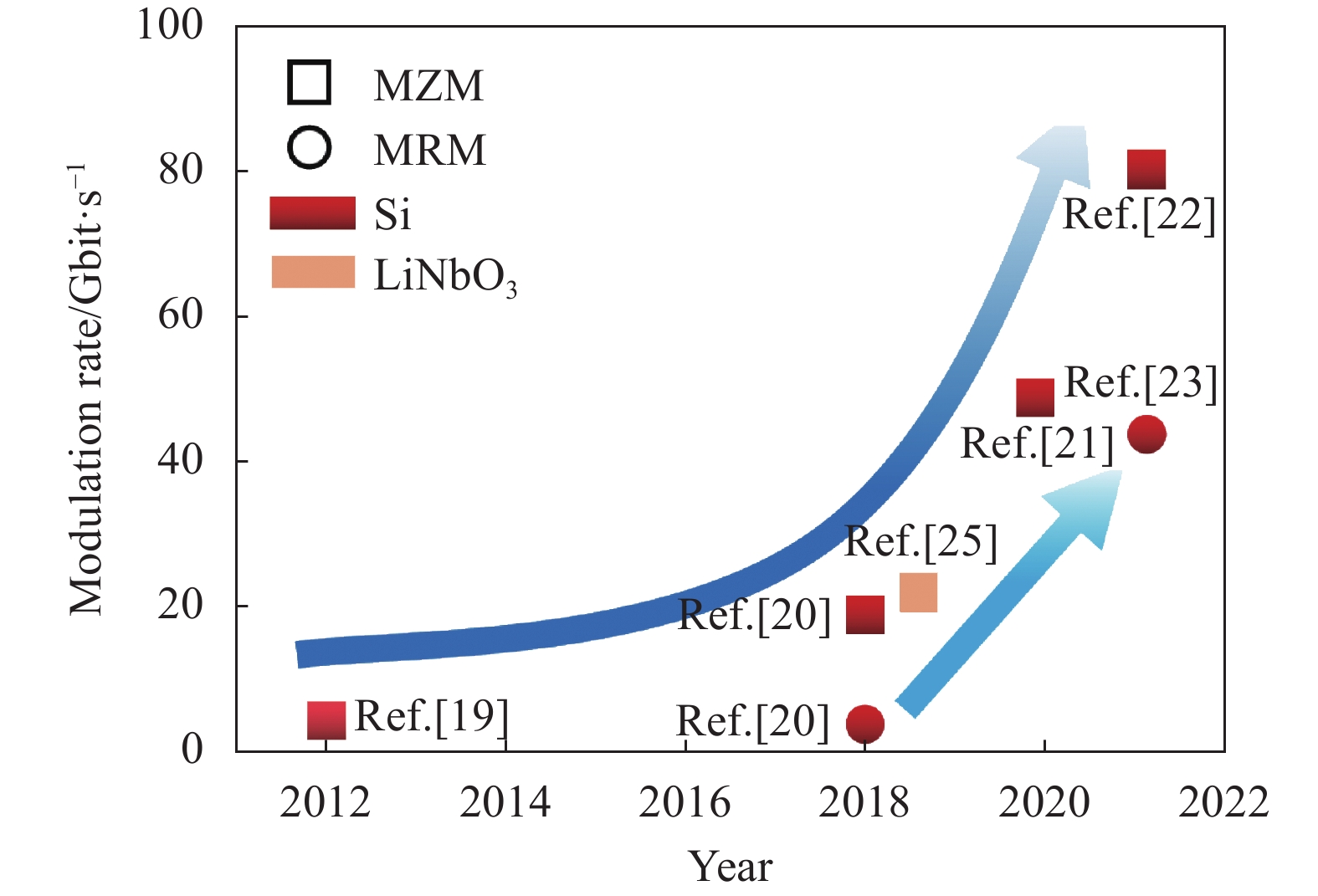
![Research progress of on-chip modulators in 2 μm waveband[19-23,25]](/richHtml/irla/2022/51/3/20220087/img_1.jpg)
![Research progress of on-chip detectors with different material systems at 2 μm waveband[27-37]](/richHtml/irla/2022/51/3/20220087/img_2.jpg)
Fig. 2. Research progress of on-chip detectors with different material systems at 2 μm waveband[27-37]
Fig. 3. (a) SEM image of cascaded MMI and SEM image of a single MMI[38]; (b) Test image of cascaded MMI[38]; (c) Schematic diagram of a power beam splitter based on subwavelength grating structure[46]; (d) Experimental result of the beam splitter based on the subwavelength grating, the inset is the SEM image of the device[46]
Fig. 4. (a) and (b) are AWG electron microscope images and experimental results images based on SOI with a top silicon thickness of 500 nm, respectively[48]; (c) and (d) are AWG electron microscope images and experimental results images based on SOI with a top silicon thickness of 220 nm, respectively[50]
Fig. 5. (a)-(d) correspond to the transmission spectra of the four output ports of the mode division multiplexer TE0, TE1, TE2, and TE3, respectively[53]
Fig. 6. (a) Electron microscope and SEM of multimode waveguide grating filter[55]; (b) Transmission spectrum under different grating periods[55]
|
Table 1. Reported performance of on-chip lasers and optical amplifiers at 2 μm band
|
Table 2. Performance comparison of reported 2 μm band grating couplers
|
Table 3. Reported performance of optical switches at 2 μm waveband
|
Table 4. Application comparison of on-chip devices based on various material systems

Set citation alerts for the article
Please enter your email address


