
Younghyun Kim, Didit Yudistira, Bernardette Kunert, Marina Baryshnikova, Reynald Alcotte, Cenk Ibrahim Ozdemir, Sanghyeon Kim, Sebastien Lardenois, Peter Verheyen, Joris Van Campenhout, Marianna Pantouvaki. Monolithic GaAs/Si V-groove depletion-type optical phase shifters integrated in a 300 mm Si photonics platform[J]. Photonics Research, 2022, 10(6): 1509
- Photonics Research
- Vol. 10, Issue 6, 1509 (2022)
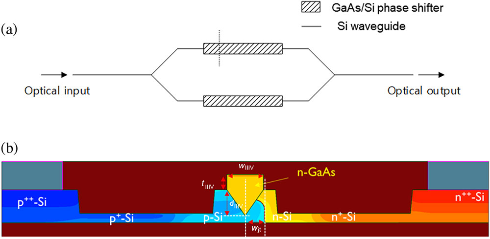
Fig. 1. (a) Schematic of a Mach–Zehnder modulator with the III–V/Si optical phase shifters in both arms. (b) Cross-section of the GaAs/Si optical phase shifter.
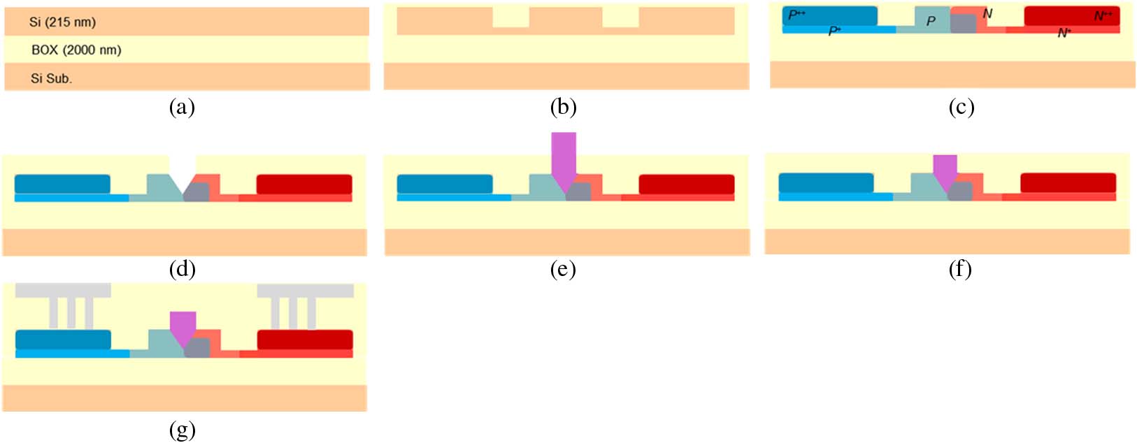
Fig. 2. Integration flow of the GaAs/Si optical phase shifter. (a) Si-on-insulator, (b) waveguide formation, (c) L-shape pn junction formation, (d) Si V-groove formation, (e) epitaxial GaAs growth on Si V-groove, (f) planarization, and (g) SiO 2
Fig. 3. (a) Cross-section of the optical phase shifter and (b) the magnified dashed yellow rectangle for GaAs/Si V-groove.
Fig. 4. EDX images of (a) Si, (b) Ga, and (c) As.
Fig. 5. Optical microscopic top-view image of the fabricated GaAs/Si V-groove lumped MZ modulators of 500-, 1000-, and 1500-μm-long optical phase shifters at both arms.
Fig. 6. Electrical characteristics of the pn junction in the GaAs/Si and Si optical phase shifters: (a) current-voltage and (b) capacitance-voltage.
Fig. 7. Bias-dependent measured spectra of the lumped MZ modulators with the 500-μm-phase shifter length: (a) the Si reference and (b) the GaAs/Si.
Fig. 8. (a) Extracted phase shift and (b) V π L
Fig. 9. Phase shifter length-dependent measured spectra of the lumped MZ modulators with 500-, 1000-, and 1500-μm phase shifter lengths: (a) the Si reference and (b) the GaAs/Si.
Fig. 10. Normalized insertion as a function of the phase shifter length for extracting the propagation loss of the GaAs/Si and the Si reference phase shifters.
Fig. 11. (a) Test site of the spiral waveguides including the GaAs/Si waveguide, the Si waveguide, and the waveguide transition. (b) The GaAs/Si waveguide region, red-colored rectangle. (c) The waveguide transition region from the Si to the GaAs/Si waveguide, blue-colored rectangle. (d) The measured transmission of the REF waveguide, Spiral 01, and Spiral 02.
Fig. 12. (a) Propagation loss of the GaAs/Si waveguide and (b) the insertion loss of the waveguide transition.
Fig. 13. (a) Optical power versus applied voltage for the OMA definition and (b) the comparison of the OMA versus the phase shifter length between the GaAs/Si and the Si modulators.
|
Table 1. Parameter Values of Waveguide Lengths and Number of Waveguide Transitions for Spiral 01 and Spiral 02

Set citation alerts for the article
Please enter your email address
© Copyright 2018-2021 | Chinese Laser Press. All Rights Reserved 沪ICP备15018463号-20