
Peng Wang, Gaofei Li, Miao Wang, Hong Li, Jing Zheng, Liyou Yang, Yigang Chen, Dongdong Li, Linfeng Lu. Numerical study of mono-crystalline silicon solar cells with passivated emitter and rear contact configuration for the efficiency beyond 24% based on mass production technology[J]. Journal of Semiconductors, 2020, 41(6): 062701
- Journal of Semiconductors
- Vol. 41, Issue 6, 062701 (2020)
Abstract
1. Introduction
The first mono-crystalline silicon solar cell with passivated emitter rear contact (PERC) configuration was proposed in 1989[
In 2019, the average mass-production efficiency of p-type mono-crystalline PERC solar cells has reached around 22%, which is 1.2% higher than that of Al-BSF solar cells[
2. Device structure and simulation parameters
The PERC solar cell is simulated by Quokka 2 software, which solves the charge carrier transport in a quasi-neutral silicon device[
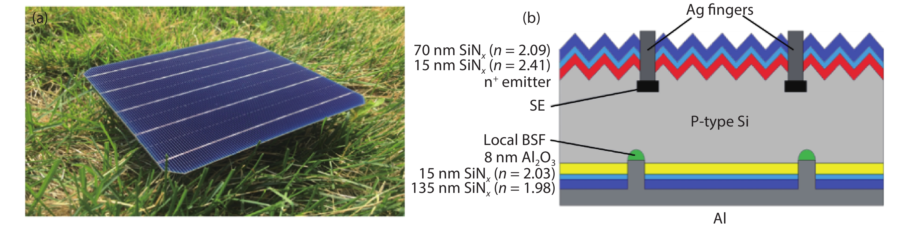
Fig. 1(a) shows a digital camera image of a PERC solar cell with five busbars from our product line. The simulation model (Fig. 1(b)) is configured based on the products. The width of simulated solar cell is 200 μm. The solar cell features a front selective emitter (SE) configuration. The emitter is passivated with a double-layered SiNx thin films, in which the refractive index (@632 nm) and thickness of the bottom SiNx are 2.41/15 nm and the top SiNx are 2.09/70 nm, respectively. Al2O3/double-layered SiNx stacked thin films are deposited on the rear side, in which the thickness of Al2O3 is 8 nm and the refractive index and thickness of SiNx are 2.03/15 nm, 1.98/135 nm, respectively. The generation profile of light to electrical carriers is simulated by Module Ray Tracer from PV Lighthouse, Sunsolve[
![]()
Figure 1.(Color online) (a) A digital camera image of a PERC solar cell with five busbars from our product line. (b) Schematic illustration of the basic PERC solar cell structure in the simulation.
Table 1 lists the initial parameters of the PERC reference cell, which includes the data acquired from the production line and literatures. Based on the data in Table 1, a 21.90% efficiency reference PERC solar cell is obtained by simulation, which is similar with the mass-produced efficiency as shown in Fig. 2.
![]()
Figure 2.The
3. Results and discussion
3.1. Surface passivation of the emitters
Based on the simulated 21.90% PERC reference solar cell, potential improvements from surface passivation, silicon wafer quality and metal grid line are studied using data from the literature to pave the way for PERC solar cells beyond 24%. In PERC solar cells, the front double-layered SiNx thin films act not only as antireflection layers but also as a passivation layer. This passivation layer has a significant increase on the electrical properties of the solar cell, especially the VOC and JSC. The passivation performance is reflected by the reverse saturation current density (J0E) in the simulated model. The relationship between the recombination current density (Jrec) and J0E is given by[
where n and p represent the concentration of electrons and holes, respectively, and ni,eff represents the effective intrinsic carrier concentration. According to the Eq. (1), reducing the J0E will lead a lower the Jrec and a better passivation performance.
In an ideal case, the relationship between VOC, JSC and Jrec can be expressed by[
where Jph is the photocurrent density, K the Boltzmann constant, T the thermodynamic temperature, q the electron charge, and v the voltage. According to the Eqs. (2) and (3), the VOC and JSC increase as the recombination current Jrec decreases. Therefore, an excellent passivation layer can effectively increase the VOC and JSC of the cell. In the reference cell, a double-layered SiNx having different refractive indices is selected as the front surface passivation layer based on our production line. Besides the double-layered SiNx, Huang et al. systematically studied the passivation mechanism and performance of stacked PECVD SiOxNy/SiNx, thermally grown SiO2/SiNx, thermally grown SiO2/ALD Al2O3/SiNx and ALD Al2O3/SiNx[
![]()
Figure 3.(Color online) The relationship between the saturation current density
Fig. 4 compares the electrical properties of the four types of stacked films (SiO2/Al2O3/SiNx, SiO2/SiNx, SiOxNy/SiNx and Al2O3/SiNx) that are used in the PERC model. The thickness and refractive index of the double-layered SiNx and the simulation parameters are consistent with the reference cell, while all SiO2, SiOxNy, Al2O3 in the four stacked films are 7 nm. It is seen that the VOC and FF are positive dependent on the J0E. Although a lower J0E can benefit photocurrent, the optical parasitic loss seems dominant and leads to decreased JSC. Eventually, the device using SiO2/SiNx has the highest efficiency of 22.22%, which is 0.32% higher than that of the reference cell, while the cell using Al2O3/SiNx has the lowest simulated efficiency of 21.35%. Therefore, in the subsequent optimization process, SiO2/SiNx stacked film is selected as the emitter passivation layer.
![]()
Figure 4.(Color online) Comparison of (a) simulated efficiency and
3.2. Quality of the silicon wafer
A silicon wafer with high carrier lifetime is of great benefit for improving solar cell efficiency. The carrier lifetime is inversely proportional to the recombination rate (R). The R, as a comprehensive result of Auger, radiative and Shockley-Read-Hall (SRH) recombination, which can be expressed as[
where RAuger is the Auger recombination rate derived from the research of Richter[
where n1 = ni,eff exp[(Et− Ei)/kT], p1 = ni,eff exp[−(Et− Ei)/kT], Et is the defect level, Ei is the intrinsic level, and τn0 and τp0 represent the lifetime of electrons and holes, respectively. τn0/p0 = (vthσNt)−1, where the average thermal motion rate vth = 1.1 × 107 cm/s, σ is the capture section of the defect recombination center for electron/hole, and Nt is the defect concentration. The last part in the Eq. (4) represents for the recombination caused by a fixed; that is, injection independent, bulk minority carrier lifetime τb,fixed.
In boron-doped p-type silicon wafers, the BO complex defect is an important SRH recombination center affecting carrier lifetime of the silicon wafer. Fig. 5 shows the carrier lifetime of p-type silicon wafer of varying resistivity under different conditions of BO complex activity. The intrinsic limit solid curve[
![]()
Figure 5.(Color online) Relationship between resistivity and carrier lifetime of silicon wafer under intrinsic limit condition and different BO deactivated processing conditions[
Based on the relationship between wafer resistivity and carrier lifetime shown in Fig. 5, the electrical performance for different wafer resistivity is simulated in Fig. 6. Furthermore, in Fig. 6, the results from Refs. [33–35] are labeled as sample As, Bs and Cs, respectively. It can be seen that the efficiencies, VOC and JSC of all samples increase with increasing wafer resistivity over the range of 0.5–1.5 Ω·cm. When the wafer resistivity increases further, VOC and JSC saturate gradually for both of Bs and Cs, while efficiencies of Bs show slight decreasing and efficiencies of Cs become saturated. These trends for efficiencies, VOC and JSC are similar with the experimental results[
![]()
Figure 6.(Color online) The electrical performance of PERC solar cells varies with the resistivity of silicon wafers under intrinsic limit and different BO deactivated processing conditions[
3.3. Metal electrodes
In the reference cell, the front grid line uses mainstream five busbars (BB) technology. The busbar width is 700 μm, while the width and pitch size of fingers are 38 and 1600 μm, respectively. The width of the busbars and the fingers are converted to a whole optical shading width of 57.7 μm with a shading factor of 0.69[
In order to further reduce the series resistance of the cell and improve efficiency, multi-busbar technology (MBB) is expected developed rapidly[
In the current industrial production of PERC solar cells, Ag paste is generally used in the front screen printing while Al paste is used on the rear side. A multilayer material with higher density and higher conductivity using nickel, copper and other metals based on the electrolysis principle is also used in the metallization scheme[
In the simulation optimization, the front grid line of PERC adopts a 12 BB design. By calculating the total optical shading area of the metal electrodes, combined with the busbar and finger width of 300 and 38 μm for 12 BB technology and the shading factor of 0.69[
Fig. 7 summarizes the three optimization steps of the PERC solar cell. The first step is the n+ emitter passivation optimization. According to different passivation layers, the cell using SiO2/SiNx has the highest simulated efficiency, followed by SiO2/Al2O3/SiNx, SiOxNy/SiNx and Al2O3/SiNx. When using a SiO2/SiNx passivation layer, the surface J0E reaches as low as 20 fA/cm2 and the cell efficiency reaches 22.22%, which is 0.32% higher than the reference cell. An optimized bulk resistivity of 1.5 Ω·cm is obtained in the second step. The star, rhombic and circle in step (2) are electrical parameters that are based on silicon wafers with carrier lifetimes of 6200, 2500 and 430 μs, respectively, which are described in Fig. 4. When the carrier lifetime is taken as 6200 μs, the simulation efficiency of the cell is 23.13%, which is considered as the limiting efficiency in this step. When the carrier lifetime is 2500 μs, the simulation efficiency of the cell is 22.98%. The third step is the optimization of the metal electrodes based on a carrier lifetime of 2500 μs. The hollow stars represent the 23.76% efficiency based on the 12 BB technology by which the shading width reduces from 57.7 to 32.6 μm. If the screen-print Ag paste is furtherly replaced by the electroplated Ni/Cu electrode with lower contact resistivity of 0.1 mΩ·cm2 and width of 32.6 μm, the efficiency can be improved to 24.04% thanks to the significant improvement of FF of up to 81.24%, while the VOC and JSC remain constant. These results are represented by solid hollow stars, as shown in Fig. 7.
![]()
Figure 7.(Color online) Simulated solar cell of a possible scenario for further PERC cell improvements. In step (1), the star, triangle, circle and rhombus points represent cells with SiO2/SiN
Based on the free energy loss analysis (FELA) simulation, Fig. 8 shows the analysis of the efficiency loss sources of PERC solar cell between the efficiency of 24.04% and the ultimate limit efficiency of 29% based on the Shockley–Queisser model[
![]()
Figure 8.(Color online) Sources of the efficiency loss between the simulated PERC solar cell with 24.04% to the limit efficiency of 29%.
4. Conclusion
A reference PERC solar cell with 21.90% efficiency is obtained from numerical simulation based on the data from the production line. Its electrical properties are well coincided with that of the practical solar cell. Based on the reference cell, the performance as a function of surface passivation, quality of silicon wafer and metal electrodes was systematically discussed. By comparing the passivation layers, SiO2/SiNx stacked thin films are considered to be the best candidates for the passivation of n+ emitters because of their low optical parasitic loss and excellent passivation properties. By considering both the passivation of BO complex and the relationship between resistivity and minority carrier lifetime, silicon wafers with resistivity of 1.5 Ω·cm and carrier lifetime of 2500 μs are preferred. For metal electrodes, the 12 BB technology and Ni/Cu electrode are employed with an optimal shading width of 32.6 μm and contact resistivity of 0.1 mΩ·cm2. Finally, a PERC model with an efficiency of 24.04% is obtained. In addition, an analysis of the efficiency loss sources from the 24.04% simulated efficiency to the 29% ultimate limit of PERC solar cell is performed. It can be seen that there is still much room for optimization in terms of surface reflection loss, absorption loss and SRH recombination loss. Therefore, this work is expected to give a guideline for the design and manufacture of high-efficiency PERC solar cells.
Acknowledgments
This work was supported by the National Natural Science Foundation of China (No. 61504155).
References
[1] A W Blakers, A Wang, A M Milne et al. 22.8% efficient silicon solar cell. Appl Phys Lett, 55, 1363(1989).
[2] S Joonwichien, S Utsunomiya, Y Kida et al. Improved rear local contact formation using Al paste containing Si for industrial PERC solar cell. IEEE J Photovolt, 8, 54(2018).
[3] A M Albadri. Characterization of Al2O3 surface passivation of silicon solar cells. TSF, 562, 451(2014).
[4] M Pawlik, J P Vilcot, M Halbwax et al. Electrical and chemical studies on Al2O3 passivation activation process. Energy Procedia, 60, 85(2014).
[5]
[6] D Inns. Understanding metal induced recombination losses in silicon solar cells with screen printed silver contacts. Energy Procedia, 98, 23(2016).
[7] N Chen, A Ebong. Towards 20% efficient industrial Al-BSF silicon solar cell with multiple busbars and fine gridlines. Sol Energy Mater Sol Cells, 146, 107(2016).
[8]
[9] B Hallam, A Herguth, P Hamer et al. Eliminating light-induced degradation in commercial p-type Czochralski silicon solar cells. Appl Sci, 8, 10(2018).
[10] A Herguth, G Hahn. Kinetics of the boron-oxygen related defect in theory and experiment. J Appl Phys, 108, 114509(2010).
[11]
[12]
[13] M Müller, G Fischer, B Bitnar et al. Loss analysis of 22% efficient industrial PERC solar cells. Energy Procedia, 124, 131(2017).
[14]
[15] A Fell. A free and fast three-dimensional/two-dimensional solar cell simulator featuring conductive boundary and quasi-neutrality approximations. IEEE Trans Electron Devices, 60, 733(2013).
[16] J A Del Alamo, R M Swanson. The physics and modeling of heavily doped emitters. IEEE Trans Electron Devices, 31, 1878(1984).
[17] R M J S C Swanson. Point-contact solar cells: modeling and experiment. Sol Cells, 17, 85(1986).
[18] R Brendel. Modeling solar cells with the dopant-diffused layers treated as conductive boundaries. Prog Photovolt: Res Appl, 20, 31(2012).
[19]
[20] A Fell, K R Mcintosh, P P Altermatt et al. Input parameters for the simulation of silicon solar cells in 2014. IEEE J Photovolt, 5, 1250(2017).
[21] B Min, M Müller, H Wagner et al. A roadmap toward 24% efficient PERC solar cells in industrial mass production. IEEE J Photovolt, 7, 1541(2017).
[22] M Ernst, D Walter, A Fell et al. Efficiency potential of p-type Al passivated perc solar cells with locally laser-doped rear contacts. IEEE J Photovolt, 6, 1(2016).
[23] W Shockley. The theory of p−n junctions in semiconductors and p−n junction transistors. Bell Syst Tech J, 28, 435(1949).
[24] P Würfel. Physics of solar cells: from principles to new concepts. Berlin: Wiley-vch(2005).
[25] H Huang, C Modanese, S Sun et al. Effective passivation of p+ and n+ emitters using SiO2/Al2O3/SiN
[26] A Kimmerle, M M Rahman, S Werner et al. Precise parameterization of the recombination velocity at passivated phosphorus doped surfaces. J Appl Phys, 119, 025706(2016).
[27] G Dingemans, W Kessels. Status and prospects of Al2O3-based surface passivation schemes for silicon solar cells. J Vac Sci Technol A, 30, 040802(2012).
[28] S W Glunz, F Feldmann. SiO2 surface passivation layers–a key technology for silicon solar cells. Sol Energy Mater Sol Cells, 185, 260(2018).
[29] Z Zhuo, Y Sannomiya, Y Kanetani et al. Interface properties of SiO
[30] A Richter, S W Glunz, F Werner et al. Improved quantitative description of Auger recombination in crystalline silicon. Phys Rev B, 86, 4172(2012).
[31] W Shockley, W Jr Read. Statistics of the recombinations of holes and electrons. Phys Rev, 87, 835(1952).
[32] R Hall. Germanium rectifier characteristics. Phys Rev, 83, 228(1951).
[33] A Richter, F Werner, A Cuevas et al. Improved parameterization of Auger recombination in silicon. Energy Procedia, 27, 88(2012).
[34] D C Walter, B Lim, J Schmidt. Realistic efficiency potential of next-generation industrial Czochralski-grown silicon solar cells after deactivation of the boron–oxygen-related defect center. Prog Photovolt: Res Appl, 24, 920(2016).
[35] J Schmidt, B Lim, D Walter et al. Impurity-related limitations of next-generation industrial silicon solar cells. IEEE J Photovolt, 3, 114(2013).
[36] F Wolny, T Weber, M Müller et al. Light induced degradation and regeneration of high efficiency Cz PERC cells with varying base resistivity. Energy Procedia, 38, 523(2013).
[37] R Woehl, M Hörteis, S Glunz. Analysis of the optical properties of screen-printed and aerosol-printed and plated fingers of silicon solar cells. Adv OptoElectron, 759340(2008).
[38] A Blakers. Shading losses of solar-cell metal grids. J Appl Phys, 71, 5237(1992).
[39] S Braun, G Micard, G Hahn. Solar cell improvement by using a multi busbar design as front electrode. Energy Procedia, 27, 227(2012).
[40] J Walter, M Tranitz, M Volk et al. Multi-wire interconnection of busbar-free solar cells. Energy Procedia, 55, 380(2014).
[41] A U Rehman, S H Lee. Review of the potential of the Ni/Cu plating technique for crystalline silicon solar cells. Materials, 7, 1318(2014).
[42] W Shockley, H J Queisser. Detailed balance limit of efficiency of p–n junction solar cells. J Appl Phys, 32, 510(1961).
[43] M J Kerr, A Cuevas, P Campbell. Limiting efficiency of crystalline silicon solar cells due to Coulomb-enhanced Auger recombination. Prog Photovolt: Res Appl Math, 11, 97(2003).
[44] A Richter, M Hermle, S W Glunz. Reassessment of the limiting efficiency for crystalline silicon solar cells. IEEE J Photovolt, 3, 1184(2013).


Set citation alerts for the article
Please enter your email address

© Copyright 2018-2021 | Chinese Laser Press. All Rights Reserved 沪ICP备15018463号-20