
E. Castro-Camus, M. Alfaro, "Photoconductive devices for terahertz pulsed spectroscopy: a review [Invited]," Photonics Res. 4, 0A36 (2016)
- Photonics Research
- Vol. 4, Issue 3, 0A36 (2016)
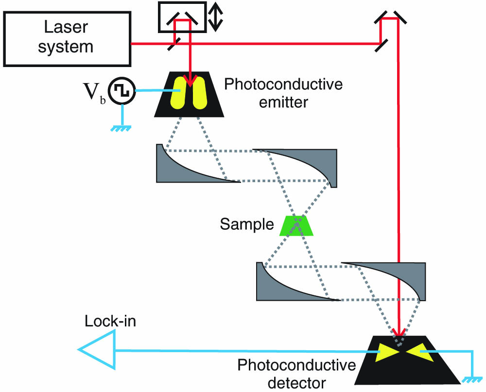
Fig. 1. Typical THz-TDS setup. The photoconductive emitter and detector are shown.
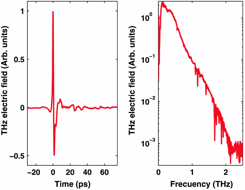
Fig. 2. Typical THz transient produced and detected by photoconductive switches (left) and its spectrum (right).
Fig. 3. Resistance and lifetime measurements for a bow-tie antenna with a 5 μm photoconductive gap. Regions (I) and (II) are marked according to the two-stage increase in the resistivity at intermediate anneal temperatures and correspond to expected optimum requirements for THz receivers and emitters, respectively. Reproduced with permission from [28], copyright 2003, American Institute of Physics.
Fig. 4. Schematic of a single nanowire photoconductive detector geometry and optical arrangement used in its characterization. The upper inset shows a THz transient measured with this device. The lower inset shows a SEM image of the device. Reproduced with permission from [56], copyright 2014, American Chemical Society.
Fig. 5. (a) Normalized luminescence distribution without bias field minus normalized luminescence distributions with bias field from a photoconductive emitter. Dark tones mark a strong field-induced reduction of the luminescence, white: enhancement of the normalized luminescence. Reproduced with permission from [62], copyright 2000, American Institute of Physics. (b) Charge distribution from a Monte Carlo simulation similar to the one presented in [65].
Fig. 6. (a) Dipole, (b) bow-tie, and (c) strip-line photoconductive antenna geometries are shown.


Set citation alerts for the article
Please enter your email address

© Copyright 2018-2021 | Chinese Laser Press. All Rights Reserved 沪ICP备15018463号-20