E. Castro-Camus1,* and M. Alfaro2
Abstract
Photoconductive switches were the key components that allowed the generation and detection of coherent broadband electromagnetic pulses at terahertz frequencies, opening the possibility for performing spectroscopy and, therefore, measuring complex dielectric properties of materials in this band, which was mostly unexplored. In this paper, we present a brief introduction to the operation principles of these devices. Subsequently, we present a review of the current state-of-the-art in this field and discuss the challenges to be faced in future development of these devices.1. INTRODUCTION
Time-domain spectroscopy (TDS) has been the key tool for exploration of the elusive portion of the electromagnetic spectrum that lies between the microwaves and the mid-infrared known as the terahertz (THz) band [1–3]. The precise definition of this band is still a matter of controversy, but, for the purposes of this publication, we will think of frequencies between and . Until the mid-1980s, the reliable generation and detection of radiation in such a band was extremely difficult. Therefore, optical, electronic, and other properties of materials at such frequencies remained unexplored. The introduction of mode-locked picosecond and subpicosecond pulsed lasers in the early 1980s opened the possibility of combining that technology with short carrier lifetime semiconductor-based optically triggered switches [4–6], which resulted in the possibility to generate and detect single-cycle radiation transients with frequency components spanning across the THz band [7]. This technique is what we know today as THz-TDS [8]. Such technique detects the time-dependent waveform of the electric field of the radiation transients instead of the frequency-dependent intensity, which is usual in traditional spectroscopy. THz-TDS allowed the characterization of complex dielectric properties of materials in this band directly from the experiment, without requiring the use of discretized Kramers–Kronig equations [9]. A few years later, nonlinear optical materials were used as an alternative to the photoconductive switches for the generation and detection of THz transients [10]. Recently, other methods based on air (or other gas) ionization also have proven useful [11], particularly when using amplified laser systems.
During the following two decades, a relatively small but active community made major improvements to many aspects of the TDS technology. In the early 2000s, commercial THz time-domain spectrometers became available. Their price has dropped dramatically since then, and their reliability and performance also have improved. This technology has also found applications in fields as distinct as solid-state physics [12–15], chemistry [16,17], biology [18–20], biochemistry [21,22], cultural heritage [23,24], and many more [25,26] that would be impractical to list exhaustively here. In this review paper, we give an overview of the evolution and state-of-the-art of photoconductive switches, which remain the most widely used emitters and detectors of THz radiation in oscillator and fiber-laser based THz systems.
2. BASICS OF THz-TDS
THz-TDS is a technique based on the generation and detection of single-cycle transients of electromagnetic radiation. A typical TDS system (Fig. 1) uses an ultrashort mode-locked laser that produces light pulses typically with durations between 10 and 100 fs. Initially, dye and Ti:sapphire lasers were used, and, more recently, rare-earth-doped fiber lasers also became popular for this purpose. The laser beam is divided into two. One of the beams is directed onto a THz emitter, which converts the ultrashort pulse into a single-cycle electromagnetic transient of duration, with a spectrum that spans across the THz band. The second part of the laser beam is directed onto a detector in order to gate it. One of the two optical paths is usually variable by using a mechanical translation stage, which allows changing the relative arrival time of the THz transient and the gating pulse to the detector. The detector produces a signal proportional to the instantaneous electric field imposed by the THz transient. By scanning the relative delay between the two beams, it is possible to map out the time-dependent form of the transient’s electric field. Typically, the emitter is biased with a square wave that alternates the polarization at a rate of a few tens of kHz inverting the polarization of the emitted THz transient; this alternation is used by the lock-in amplifier in order to filter the THz photocurrent produced in the photoconductive detector. Alternatively, the bias can be a DC field, and an optical chopper can be placed before the laser beam reaches the photoconductive emitter in order to reference the lock-in amplifier.
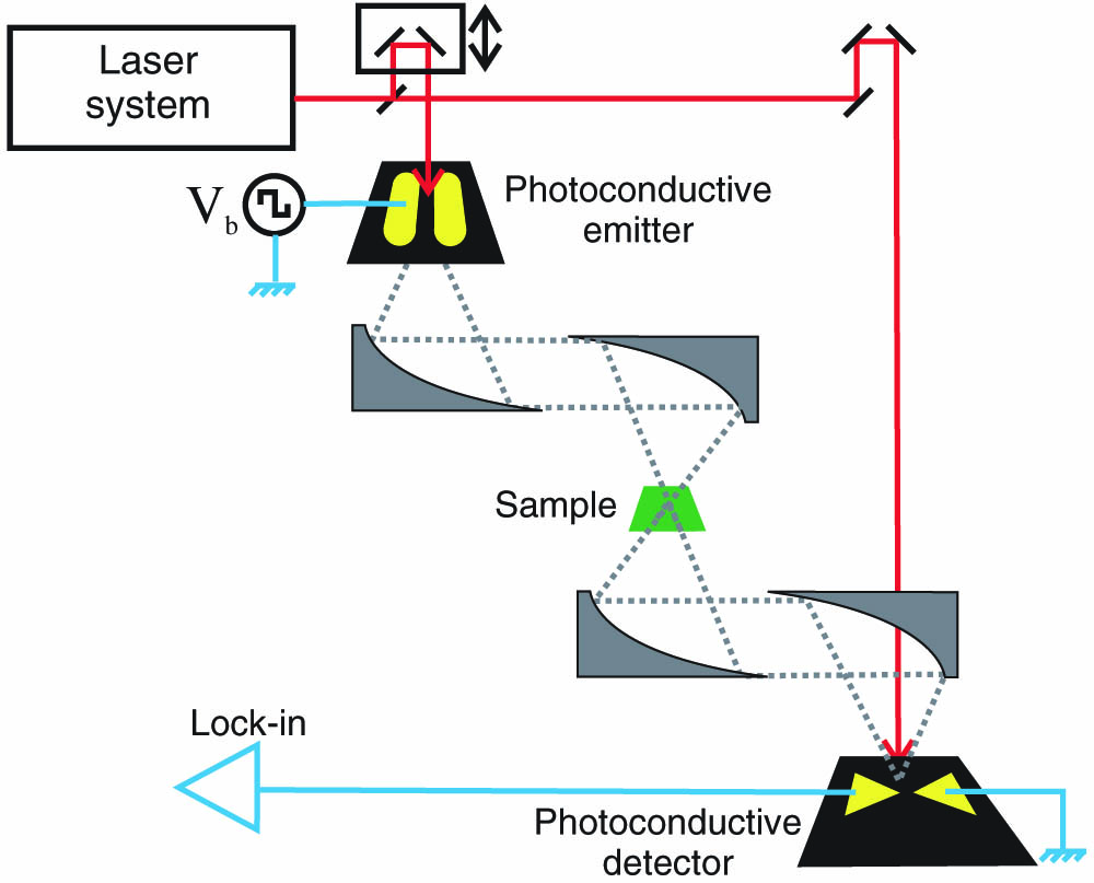
Figure 1.Typical THz-TDS setup. The photoconductive emitter and detector are shown.
In order to improve the THz coupling in and out of the THz devices, many times silicon hemispherical or hyperhemispherical lenses are attached to the substrate on the opposite surface to the contacts. These lenses help to collimate the emission and to collect the radiation in the detectors.
A. Photoconductive Switches as Emitters
A photoconductive emitter is a device made of two metallic contacts on a semiconductor substrate. For the purposes of this section, we will think of a high-resistivity semiconductor (a more detailed discussion of the role of the material properties will be given in Section 3 as well as the influence of the contact geometry in Section 4). A bias voltage is applied between the two contacts, which produces a negligible current because of the high resistivity of the semiconductor. When an ultrashort laser pulse is shone on the gap between the contacts, photocarriers are generated in the material, increasing the conductivity of the material in the subpicosecond time scale. The conductivity subsequently decreases because of recombination, trapping, or momentum scattering of the carriers in the subpicosecond to nanosecond time scale depending on the properties of the semiconductor. The current transient resulting from the sudden change in conductivity and the applied bias field produces an electromagnetic transient such as the one shown in Fig. 2.

Figure 2.Typical THz transient produced and detected by photoconductive switches (left) and its spectrum (right).
B. Photoconductive Switches as Detectors
A photoconductive detector is also a semiconductor device made of two metallic contacts with diverse geometries deposited on a high-dark-resistivity semiconductor separated by a few micrometers, typically between 1 and 50 μm. Photoconductive switches are usually not biased when used as detectors. In this case, the photoconductivity rises transitorily in a similar fashion to the emitters, but the photocarriers are accelerated by the electric field of the incoming THz transient. Although photoconductive detectors can operate in integrating, direct, or an intermediate sampling mode [27], in this section we will assume that they operate in the direct mode, which is the most widely used. Namely, the carrier lifetime is shorter than the duration of the THz transient. Therefore, the photoinduced conductivity of the detector remains “high” only for a short fraction of the THz transient, which at its time means that the current induced in the device is directly proportional to the nearly instantaneous electric field at the photoexcitation time.
For photoconductive detection, an ultrafast laser pulse and a THz single-cycle electromagnetic transient are focused synchronously on the gap between the contacts of the detector. The ultrafast laser pulse is absorbed by the semiconductor generating electron-hole pairs and therefore increasing its conductivity. In the case of direct sampling, the semiconductor remains conductive for a short period only () [28]. The comparatively slow electric field of the THz transient is nearly constant in this time scale. Therefore the current induced between the two contacts of the detector is proportional only to the electric field at the time when the photoconductivity is high. By varying the relative arrival time of the THz transient and the optical pulse, the entire waveform of the THz transient can be mapped out.
3. MATERIALS
As described in the previous section, photoconductive switches can be used as emitters and detectors. Ideally, a photoconductive switch should have as low dark conductivity, as high carrier mobility, and as short carrier lifetime as possible. However, in real semiconductors, there are trade-offs among these three characteristics. The optimal balance between these properties are different for emitters and detectors [29]. While the contrast between the dark and illuminated conductivity is important in both cases [30], a short carrier lifetime tends to be more important for detectors [31,32], at least in direct sampling mode, and a high carrier mobility is more important for emitters even if their lifetime is not as short [33–35].
As mentioned earlier, direct sampling detectors require a short carrier lifetime in order to have a time-dependent photoconductivity that resembles a Dirac-delta function. This means that it remains conductive for a period much shorter than the duration of the THz transient, which, at its time, means that the current produced between the contacts is proportional to the instantaneous electric field. The first THz photoconductive detector was fabricated by irradiating an epitaxial layer of Si grown on sapphire with ions [6]. The irradiation with ions produced defects in the crystal lattice that acted as traps, effectively reducing the free-carrier lifetime in the material at the cost of lowering the mobility. In the following years, Si was replaced by gallium arsenide grown epitaxially at low temperatures () followed by in situ annealing; in this case, the low temperature produces defects in the crystal lattice that are selectively removed by the annealing process. The annealing increases the dark resistance while maintaining a short carrier lifetime [28]. GaAs has higher mobility than Si, producing better results. Low-temperature GaAs (LT-GaAs) is still the most widely used material for photoconductive devices [31,36–38]; however, its fabrication has two major disadvantages. First, the semiconductor properties are not reproducible. Two wafers grown under the same conditions, at least nominally, even in the same reactor, present very different characteristics, particularly in terms of carrier lifetime and dark resistance. Second, the growth of high-quality LT-GaAs is still performed in molecular beam epitaxy machines; this method is too expensive for large-scale industrial production of THz devices. Perhaps one of the breakthroughs in the use of LT-GaAs was the report by Gregory et al. [28], where it was found that the fine control post-growth annealing temperature is critical in defining the properties of the resulting sample (see Fig. 3).
Figure 3.Resistance and lifetime measurements for a bow-tie antenna with a 5 μm photoconductive gap. Regions (I) and (II) are marked according to the two-stage increase in the resistivity at intermediate anneal temperatures and correspond to expected optimum requirements for THz receivers and emitters, respectively. Reproduced with permission from [28], copyright 2003, American Institute of Physics.
Various approaches also have been taken in order to eliminate the need for LT growth. The inclusion of nanostructures that reduce the lifetime without sacrificing the mobility [39–41], the use of ion implantation in materials as varied as GaAs:C [42], GaAs:As [43,44], InGaAs:Fe [45], and InP:Fe [46] have shown promising results in fabricating materials with more reproducible properties.
One advantage of GaAs is that its bandgap () is ideal for excitation by Ti:sapphire lasers, typically at wavelengths in the vicinity of 800 nm. However, in recent years, Er:fiber () and Yb:fiber () lasers have shown important advantages. Such lasers are more robust, portable, stable, require almost no maintenance, and are significantly cheaper than Ti:sapphire ones. Unfortunately, GaAs-based photoconductive switches are incompatible with such wavelengths unless inefficient, two-photon excitation is used [37]. Therefore, alternative materials that can be used for the various laser wavelengths available have been explored. With the requirement of narrower bandgap materials in the 0.8–1.2 eV region, additional challenges arise, in particular these materials have larger thermal carrier populations; therefore, high dark resistivities are more difficult to achieve. Various materials have been introduced for this application such as LT-grown InGaAs/AlInAs heterostructures [40,41], Be-doped InGaAs [47], InGaAs quantum dots [48], and GaAsBi [49,50].
Additional materials showing potential for photoconductive switch fabrication are HgCdTe [51], SiC and ZnSe [52], graphene [53,54], and other 2D materials [55]. Even single-semiconductor nanoparticle-based devices [56] have been reported. In particular, the introduction of the single-nanowire photoconductive detector, shown in Fig. 4, is a significant contribution. This kind of device opens the possibility of further miniaturization and creation of complex THz-integrated circuits and integrated quasi-optical systems.
Figure 4.Schematic of a single nanowire photoconductive detector geometry and optical arrangement used in its characterization. The upper inset shows a THz transient measured with this device. The lower inset shows a SEM image of the device. Reproduced with permission from [56], copyright 2014, American Chemical Society.
Besides the previously mentioned developments, the inclusion of antireflection coatings for the laser pulse [57] and THz radiation [58] on the semiconductor surfaces as well as other layered structures that confine the laser light [59,60] in the vicinity of the contacts have provided improvements to the performance of these devices. The post-growth chemical surface passivation of the semiconductor is another procedure that was found to improve the performance of these devices [57,61].
For over a decade now, enormous effort has been invested to understand the carrier dynamics in the semiconductor of a photoconductive switch in order to provide feedback to the semiconductor and device fabricators aiming to improve their performance. Experiments that image the photoluminescence and therefore the distribution of photocarriers were performed [62], showing that the transient electron-hole separation that generates the THz radiation is more complex than a simplistic dipole formation [see Fig. 5(a)]. Some band-transport [63,64] models were implemented, followed by Monte Carlo [65,66] models that track the motion of individual carriers in large ensembles, taking into account the local conditions of each one of them, predicting the waveform and spectra as well as providing information about the evolution of the charge distribution with outstanding accuracy [see Fig. 5(b)]. These models explained and predicted the effect of aspects such as bias-field distribution [67] and screening [68,69], anode-enhanced emission [65], free-carrier lifetime [66], trap density saturation in receivers [70], temperature dependence of the emission [71], and even the effect of co-propagation of the gating and THz radiation in a detector [72].
Figure 5.(a) Normalized luminescence distribution without bias field minus normalized luminescence distributions with bias field from a photoconductive emitter. Dark tones mark a strong field-induced reduction of the luminescence, white: enhancement of the normalized luminescence. Reproduced with permission from [62], copyright 2000, American Institute of Physics. (b) Charge distribution from a Monte Carlo simulation similar to the one presented in [65].
4. CONTACT GEOMETRIES
Contacts play a role just as important as the semiconductor they are deposited on. Their global geometry, in the few hundreds of micrometers to a few millimeter length scale, acts as an electromagnetic antenna, defining to a good extent the coupling between the free-space electromagnetic field at THz frequencies and the photocurrent flowing between them. The contact designs first introduced were the dipole, strip-line, and bow-tie geometries shown in Fig. 6 [73]. These designs showed some differences in their total efficiency, spectral response, radiation patterns, and the linear polarization they produce or detect [74,75]. In recent years, a plethora of novel contact designs have been introduced, which improve specific aspects of the photoconductive switches’ performance or even introduce new functionalities not previously available for these devices.
Figure 6.(a) Dipole, (b) bow-tie, and (c) strip-line photoconductive antenna geometries are shown.
An important improvement in the case of emitters came with the use of interdigitated contacts [34,76,77], which increases in the effective gap area. With the availability of fabrication methods capable of producing nanometric features, nanofinger structures that can simultaneously act as contacts and plasmonic guides of the laser photons have been introduced [78–80]; this means that photons are efficiently coupled into the semiconductor in the vicinity of the contacts [81], increasing their probability of reaching a contact instead of recombining, getting trapped, or drifting away from the surface and, therefore, of the contacts. Experimental studies have demonstrated a 50 times power improvement for THz emitters and 30 times improvement in the signal detected by photoconductive switches that incorporate plasmonic contacts [79]. Recent improvements on this include the fabrication of 3D plasmonic structures, which incorporate contacts that are not only deposited on the flat surface of the semiconductor but built into it, reaching an impressive 7.5% in laser-to-THz power conversion efficiency [82].
A more traditional bow-tie photoconductive emitter was also studied, which incorporates silver nano-islands on the semiconductor surface between the contacts, showing plasmonic-induced performance enhancement as well [83]. The plasmon confinement of the laser photons also has been demonstrated as a mechanism to improve two-photon absorption in GaAs and other relatively large bandgap materials when using fiber lasers [84]. Some recent publications on these nanopatterned contacts attribute better bias field distribution, which also favors the high-power emission than it does in conventional contacts [85]. Additionally, studies report that the proximity of the carriers to the contacts in these structures limits their transit time to the sub-picosecond regime, removing the need for short-carrier-lifetime semiconductor materials [78,86].
In addition to improving the emission and detection efficiencies, there have been significant efforts to design and fabricate photoconductive switches with additional capabilities. An example of this is the creation of detectors and emitters able to produce and detect different polarizations. The inclusion of three [87–89] or four [90] contacts in photoconductive detectors opened the possibility to detect the full polarization state of THz transients by measuring currents proportional to two different projections of the THz electric field. This implies that the information collected in a THz transient measurement is doubled, containing the spectral amplitude and phase of both components, which, in time, allows the unambiguous characterization of anisotropic samples such as birefringent, optically active, or dichroic materials [91]. An elegant four-contact emitter design was also introduced, which allowed linear and circular polarization modulation [92] when combined with an appropriate Si prism. Other designs have been introduced for the generation of radially and azimuthally “polarized” electromagnetic modes [93,94].
5. PERSPECTIVES AND FINAL REMARKS
THz photoconductive switch technology has significantly matured in the last 15 years. Devices compatible with laser technology from 800 to 1550 nm have been demonstrated. The need for short-carrier-lifetime semiconductors is being addressed with LT-growth, ion implantation, heterostructures, nanoparticle inclusion, and other approaches. The design of innovative contact geometries is also showing promising results, improving the emission and detection efficiencies, expanding the polarization and electromagnetic modes that can be produced and detected, and probably making the requirement of short carrier lifetime unnecessary. Miniaturization of the devices is reaching the level in which single-nanoparticle switches have been tested, opening the possibility of incorporating full THz systems in microcircuits or micrometric optical setups. However, commercially available devices are still relatively expensive. The semiconductors they are being made of are still difficult to grow, and plasmonic contacts require expensive high-resolution fabrication techniques such as electron beam lithography. Improvements in the polarization resolution of photoconductive detectors could open the possibility of performing THz vibrational-circular-dichroism spectroscopy, which promises to reveal key information about chiral biomolecules such as proteins and nucleic acids [95,96].
Although the prices of commercial THz time-domain systems have dropped dramatically during the same 15-year period, many potential applications of TDS in industry, biology, medicine, and other areas are not viable, owing to the cost of this equipment. Of course, a significant part of the cost of a TDS system comes from the ultrashort laser, but economical alternatives are being explored [97]. However, the second most significant component in terms of price are the photoconductive devices. Exciting new ideas in terms of improvement of these devices are emerging every day, but we believe the most important challenge faced by the photoconductive switch development community in this moment is finding ways of producing high-performance devices at low costs and large scales. The introduction of high-quality crystal growth techniques such as atomic layer deposition and of extreme-UV photolithography could become the key for this in the near future.
ACKNOWLEDGMENT
Acknowledgment. The authors would like to thank Centro de Investigaciones en Optica A.C. for payment of the article processing charge.
References
[1] J. M. Chamberlain. Where optics meets electronics: recent progress in decreasing the terahertz gap. Philos. Trans. R. Soc. A, 362, 199-213(2004).
[2] M. Tonouchi. Cutting-edge terahertz technology. Nat. Photonics, 1, 97-105(2007).
[3] P. U. Jepsen, D. G. Cooke, M. Koch. Terahertz spectroscopy and imaging—modern techniques and applications. Laser Photon. Rev., 5, 124-166(2011).
[4] D. H. Auston, P. R. Smith. Generation and detection of millimeter waves by picosecond photoconductivity. Appl. Phys. Lett., 43, 631-633(1983).
[5] D. H. Auston. Impulse-response of photoconductors in transmission-lines. IEEE J. Quantum Electron., 19, 639-648(1983).
[6] D. H. Auston, K. P. Cheung, P. R. Smith. Picosecond photoconducting Hertzian dipoles. Appl. Phys. Lett., 45, 284-286(1984).
[7] M. Tani, K. Yamamoto, E. S. Estacio, C. T. Que, H. Nakajima, M. Hibi, F. Miyamaru, S. Nishizawa, M. Hangyo. Photoconductive emission and detection of terahertz pulsed radiation using semiconductors and semiconductor devices. J. Infrared Millimeter Terahertz Waves, 33, 393-404(2012).
[8] K. P. Cheung, D. H. Auston. A novel technique for measuring far-infrared absorption and dispersion. Infrared Phys., 26, 23-27(1986).
[9] L. Duvillaret, F. Garet, J.-L. Coutaz. A reliable method for extraction of material parameters in terahertz time-domain spectroscopy. IEEE J. Sel. Top. Quantum Electron., 2, 739-746(1996).
[10] D. H. Auston, M. C. Nuss. Electrooptic generation and detection of femtosecond electrical transients. IEEE J. Quantum Electron., 24, 184-197(1988).
[11] J. Dai, J. Liu, X.-C. Zhang. Terahertz wave air photonics: terahertz wave generation and detection with laser-induced gas plasma. IEEE J. Sel. Top. Quantum Electron., 17, 183-190(2011).
[12] R. Huber, F. Tauser, A. Brodschelm, M. Bichler, G. Abstreiter, A. Leitenstorfer. How many-particle interactions develop after ultrafast excitation of an electron-hole plasma. Nature, 414, 286-289(2001).
[13] C. Kübler, H. Ehrke, R. Huber, R. Lopez, A. Halabica, J. R. F. Haglund, A. Leitenstorfer. Coherent structural dynamics and electronic correlations during an ultrafast insulator-to-metal phase transition in vo2. Phys. Rev. Lett., 99, 116401(2007).
[14] L. Ozyuzer, A. E. Koshelev, C. Kurter, N. Gopalsami, Q. Li, M. Tachiki, K. Kadowaki, T. Yamamoto, H. Minami, H. Yamaguchi, T. Tachiki, K. E. Gray, W. K. Kwok, U. Welp. Emission of coherent THz radiation from superconductors. Science, 318, 1291-1293(2007).
[15] J. Lloyd-Hughes, M. Failla, J. Ye, S. Jones, K. Teo, C. Jagadish. Interfacial and bulk polaron masses in zn1- xmgxo/zno heterostructures examined by terahertz time-domain cyclotron spectroscopy. Appl. Phys. Lett., 106, 202103(2015).
[16] B. Fischer, M. Hoffmann, H. Helm, G. Modjesch, P. U. Jepsen. Chemical recognition in terahertz time-domain spectroscopy and imaging. Semicond. Sci. Technol., 20, S246(2005).
[17] M. B. Johnston, L. M. Herz, A. L. T. Khan, A. Köhler, A. G. Davies, E. H. Linfield. Low-energy vibrational modes in phenylene oligomers studied by THz time-domain spectroscopy. Chem. Phys. Lett., 377, 256-262(2003).
[18] E. Castro-Camus, M. Palomar, A. Covarrubias. Leaf water dynamics of arabidopsis thaliana monitored in-vivo using terahertz time-domain spectroscopy. Sci. Rep., 3, 2910(2013).
[19] R. Gente, N. Born, N. Voß, W. Sannemann, J. Léon, M. Koch, E. Castro-Camus. Determination of leaf water content from terahertz time-domain spectroscopic data. J. Infrared Millimeter Terahertz Waves, 34, 316-323(2013).
[20] R. M. Woodward, B. E. Cole, V. P. Wallace, R. J. Pye, D. D. Arnone, E. H. Linfield, M. Pepper. Terahertz pulse imaging in reflection geometry of human skin cancer and skin tissue. Phys. Med. Biol., 47, 3853-3863(2002).
[21] B. Born, M. Havenith. Terahertz dance of proteins and sugars with water. J. Infrared Millimeter Terahertz Waves, 30, 1245-1254(2009).
[22] R. J. Falconer, A. G. Markelz. Terahertz spectroscopic analysis of peptides and proteins. J. Infrared Millimeter Terahertz Waves, 33, 973-988(2012).
[23] K. Fukunaga, N. Sekine, I. Hosako, N. Oda, H. Yoneyama, T. Sudou. Real-time terahertz imaging for art conservation science. J. Eur. Opt. Soc., 3, 08027(2008).
[24] K. Krügener, M. Schwerdtfeger, S. Busch, A. Soltani, E. Castro-Camus, M. Koch, W. Viöl. Terahertz meets sculptural and architectural art: Evaluation and conservation of stone objects with t-ray technology. Sci. Rep., 5, 14842(2015).
[25] C. Riek, D. Seletskiy, A. Moskalenko, J. Schmidt, P. Krauspe, S. Eckart, S. Eggert, G. Burkard, A. Leitenstorfer. Direct sampling of electric-field vacuum fluctuations. Science, 350, 420-423(2015).
[26] M. Schwerdtfeger, S. Lippert, M. Koch, A. Berg, S. Katletz, K. Wiesauer. Terahertz time-domain spectroscopy for monitoring the curing of dental composites. Biomed. Opt. Express, 3, 2842-2850(2012).
[27] E. Castro-Camus, L. Fu, J. Lloyd-Hughes, H. H. Tan, C. Jagadish, M. B. Johnston. Photoconductive response correction for detectors of terahertz radiation. J. Appl. Phys., 104, 053113(2008).
[28] I. S. Gregory, C. Baker, W. R. Tribe, M. J. Evans, H. E. Beere, E. H. Linfield, A. G. Davies, M. Missous. High resistivity annealed low-temperature GaAs with 100 fs lifetimes. Appl. Phys. Lett., 83, 4199-4201(2003).
[29] Y. Kamo, S. Kitazawa, S. Ohshima, Y. Hosoda. Highly efficient photoconductive antennas using optimum low-temperature-grown GaAs layers and si substrates. Jpn. J. Appl. Phys., 53, 032201(2014).
[30] W. Hou, L. Shi. An lt-GaAs terahertz photoconductive antenna with high emission power, low noise, and good stability. IEEE Trans. Electron Devices, 60, 1619-1624(2013).
[31] Y. C. Shen, P. C. Upadhya, H. E. Beere, E. H. Linfield, A. G. Davies, I. S. Gregory, C. Baker, W. R. Tribe, M. J. Evans. Generation and detection of ultrabroadband terahertz radiation using photoconductive emitters and receivers. Appl. Phys. Lett., 85, 164-166(2004).
[32] N. Wang, M. Jarrahi. Noise analysis of photoconductive terahertz detectors. J. Infrared Millimeter Terahertz Waves, 34, 519-528(2013).
[33] M. Venkatesh, K. Rao, T. Abhilash, S. Tewari, A. Chaudhary. Optical characterization of GaAs photoconductive antennas for efficient generation and detection of terahertz radiation. Opt. Mater., 36, 596-601(2014).
[34] P. J. Hale, J. Madeo, C. Chin, S. S. Dhillon, J. Mangeney, J. Tignon, K. M. Dani. 20 THz broadband generation using semi-insulating GaAs interdigitated photoconductive antennas. Opt. Express, 22, 26358-26364(2014).
[35] S. A. F. Sirbu, M. Lepaul. Coupling 3-d Maxwell’s and Boltzmann’s equations for analyzing a terahertz photoconductive switch. IEEE Trans. Microwave Theory Tech., 53, 2991-2998(2005).
[36] Y. C. Shen, P. C. Upadhya, E. H. Linfield, H. E. Beere, A. G. Davies. Ultrabroadband terahertz radiation from low-temperature-grown GaAs photoconductive emitters. Appl. Phys. Lett., 83, 3117-3119(2003).
[37] M. Tani, K.-S. Lee, X.-C. Zhang. Detection of terahertz radiation with low-temperature-grown GaAs-based photoconductive antenna using 1.55 ?m probe. Appl. Phys. Lett., 77, 1396-1398(2000).
[38] J. Zhang, Y. Hong, S. Braunstein, K. Shore. Terahertz pulse generation and detection with lt-GaAs photoconductive antenna. IEE Proceedings of Optoelectronics, 151, 98-101(2004).
[39] J. F. O’Hara, J. M. O. Zide, A. C. Gossard, A. J. Taylor, R. D. Averitt. Enhanced terahertz detection via ErAs:GaAs nanoisland superlattices. Appl. Phys. Lett., 88, 251119(2006).
[40] R. J. Dietz, B. Globisch, H. Roehle, D. Stanze, T. Göbel, M. Schell. Influence and adjustment of carrier lifetimes in InGaAs/InAlAs photoconductive pulsed terahertz detectors: 6 THz bandwidth and 90db dynamic range. Opt. Express, 22, 19411-19422(2014).
[41] I. Kostakis, D. Saeedkia, M. Missous. Terahertz generation and detection using low temperature grown InGaAs-InAlAs photoconductive antennas at 1.55 pulse excitation. IEEE Trans. Terahertz Sci. Technol., 2, 617-622(2012).
[42] A. Singh, S. Pal, H. Surdi, S. S. Prabhu, S. Mathimalar, V. Nanal, R. G. Pillay, G. Döhler. Carbon irradiated semi insulating GaAs for photoconductive terahertz pulse detection. Opt. Express, 23, 6656-6661(2015).
[43] T.-A. Liu, M. Tani, M. Nakajima, M. Hangyo, C.-L. Pan. Ultrabroadband terahertz field detection by photoconductive antennas based on multi-energy arsenic-ion-implanted GaAs and semi-insulating GaAs. Appl. Phys. Lett., 83, 1322-1324(2003).
[44] J. Lloyd-Hughes, E. Castro-Camus, M. D. Fraser, C. Jagadish, M. B. Johnston. Carrier dynamics in ion-implanted GaAs studied by simulation and observation of terahertz emission. Phys. Rev. B, 70, 235330(2004).
[45] M. Suzuki, M. Tonouchi. Fe-implanted InGaAs photoconductive terahertz detectors triggered by 1.56 m femtosecond optical pulses. Appl. Phys. Lett., 86, 163504(2005).
[46] E. Castro-Camus, J. Lloyd-Hughes, L. Fu, H. H. Tan, C. Jagadish, M. B. Johnston. An ion-implanted InP receiver for polarization resolved terahertz spectroscopy. Opt. Express, 15, 7047-7057(2007).
[47] A. Takazato, M. Kamakura, T. Matsui, J. Kitagawa, Y. Kadoya. Terahertz wave emission and detection using photoconductive antennas made on low-temperature-grown InGaAs with 1.56 m pulse excitation. Appl. Phys. Lett., 91, 011102(2007).
[48] D. G. Cooke, F. A. Hegmann, Y. I. Mazur, W. Q. Ma, X. Wang, Z. M. Wang, G. J. Salamo, M. Xiao, T. D. Mishima, M. B. Johnson. Anisotropic photoconductivity of InGaAs quantum dot chains measured by terahertz pulse spectroscopy. Appl. Phys. Lett., 85, 3839-3841(2004).
[49] A. Arlauskas, P. Svidovsky, K. Bertulis, R. Adomavičius, A. Krotkus. GaAsBi photoconductive terahertz detector sensitivity at long excitation wavelengths. Appl. Phys. Express, 5, 022601(2012).
[50] K. Bertulis, A. Krotkus, G. Aleksejenko, V. Pacebutas, R. Adomavicius, G. Molis, S. Marcinkevicius. GaBiAs: a material for optoelectronic terahertz devices. Appl. Phys. Lett., 88, 201112(2006).
[51] M. Kinch, S. Borrello, B. Breazeale, A. Simmons. Geometrical enhancement of hgcdte photoconductive detectors. Infrared Phys., 17, 137-145(1977).
[52] X. Ropagnol, M. Bouvier, M. Reid, T. Ozaki. Improvement in thermal barriers to intense terahertz generation from photoconductive antennas. J. Appl. Phys., 116, 043107(2014).
[53] N. Hunter, A. S. Mayorov, C. D. Wood, C. Russell, L. Li, E. H. Linfield, A. G. Davies, J. E. Cunningham. On-chip picosecond pulse detection and generation using graphene photoconductive switches. Nano Lett., 15, 1591-1596(2015).
[54] A. Cabellos-Aparicio, I. Llatser, E. Alarcon, A. Hsu, T. Palacios. Use of terahertz photoconductive sources to characterize tunable graphene rf plasmonic antennas. IEEE Trans. Nanotechnol., 14, 390-396(2015).
[55] F. Koppens, T. Mueller, P. Avouris, A. Ferrari, M. Vitiello, M. Polini. Photodetectors based on graphene, other two-dimensional materials and hybrid systems. Nat. Nanotechnol., 9, 780-793(2014).
[56] K. Peng, P. Parkinson, L. Fu, Q. Gao, N. Jiang, Y.-N. Guo, F. Wang, H. J. Joyce, J. L. Boland, H. H. Tan, C. Jagadish, M. B. Johnston. Single nanowire photoconductive terahertz detectors. Nano Lett., 15, 206-210(2015).
[57] C. Headley, L. Fu, P. Parkinson, X. L. Xu, J. Lloyd-Hughes, C. Jagadish, M. B. Johnston. Improved performance of GaAs-based terahertz emitters via surface passivation and silicon nitride encapsulation. IEEE J. Sel. Top. Quantum Electron., 17, 17-21(2011).
[58] F. D. Brunner, T. Feurer. Antireflection coatings optimized for single-cycle THz pulses. Appl. Opt., 52, 3829-3832(2013).
[59] O. Mitrofanov, I. Brener, T. S. Luk, J. L. Reno. Photoconductive terahertz near-field detector with a hybrid nanoantenna array cavity. ACS Photon., 2, 1763-1768(2015).
[60] M. Kozub, K. Nishisaka, T. Maemoto, S. Sasa, K. Takayama, M. Tonouchi. Reflection layer mediated enhancement of terahertz radiation utilizing heavily-doped InAs thin films. J. Infrared Millimeter Terahertz Waves, 36, 423-429(2015).
[61] J. Lloyd-Hughes, S. K. E. Merchant, L. Fu, H. H. Tan, C. Jagadish, E. Castro-Camus, M. B. Johnston. Influence of surface passivation on ultrafast carrier dynamics and terahertz radiation generation in GaAs. Appl. Phys. Lett., 89, 232102(2006).
[62] M. Bieler, G. Hein, K. Pierz, U. Siegner, M. Koch. Spatial pattern formation of optically excited carriers in photoconductive switches. Appl. Phys. Lett., 77, 1002-1004(2000).
[63] Z. Piao, M. Tani, K. Sakai. Carrier dynamics and terahertz radiation in photoconductive antennas. Jpn. J. Appl. Phys., 39, 96-100(2000).
[64] M. Koch, M. Bieler, G. Hein, K. Pierz, U. Siegner. Photoconductive switches: the role of spatial effects in carrier dynamics. Phys. Status Solidi B, 221, 429-433(2000).
[65] E. Castro-Camus, J. Lloyd-Hughes, M. B. Johnston. Three-dimensional carrier-dynamics simulation of terahertz emission from photoconductive switches. Phys. Rev. B, 71, 195301(2005).
[66] J. Lloyd-Hughes, E. Castro-Camus, M. B. Johnston. Simulation and optimisation of terahertz emission from InGaAs and InP photoconductive switches. Solid State Commun., 136, 595-600(2005).
[67] M. Xu, M. Mittendorff, R. J. B. Dietz, H. Knzel, B. Sartorius, T. Gbel, H. Schneider, M. Helm, S. Winnerl. Terahertz generation and detection with InGaAs-based large-area photoconductive devices excited at 1.55 m. Appl. Phys. Lett., 103, 251114(2013).
[68] D. S. Kim, D. S. Citrin. Coulomb and radiation screening in photoconductive terahertz sources. Appl. Phys. Lett., 88, 161117(2006).
[69] E. Moreno, M. Pantoja, F. Ruiz, J. Roldn, S. Garca. On the numerical modeling of terahertz photoconductive antennas. J. Infrared Millimeter Terahertz Waves, 35, 432-444(2014).
[70] E. Castro-Camus, M. Johnston, J. Lloyd-Hughes. Simulation of fluence-dependent photocurrent in terahertz photoconductive receivers. Semicond. Sci. Technol., 27, 115011(2012).
[71] F. Zangeneh-Nejad, N. Barani, R. Safian. Temperature dependence of electromagnetic radiation from terahertz photoconductive antennas. Microwave Opt. Technol. Lett., 57, 2475-2479(2015).
[72] V. Malevich, G. Sinitsyn. Response speed of terahertz photoconductive receiver antennas when excited by femtosecond laser pulses. J. Appl. Spectrosc., 80, 289-293(2013).
[73] M. Tani, S. Matsuura, K. Sakai, S. Nakashima. Emission characteristics of photoconductive antennas based on low-temperature-grown GaAs and semi-insulating GaAs. Appl. Opt., 36, 7853-7859(1997).
[74] R. Yano, H. Gotoh, Y. Hirayama, S. Miyashita, Y. Kadoya, T. Hattori. Terahertz wave detection performance of photoconductive antennas: role of antenna structure and gate pulse intensity. J. Appl. Phys., 97, 103103(2005).
[75] J. Vanrudd, J. L. Johnson, D. M. Mittleman. Cross-polarized angular emission patterns from lens-coupled terahertz antennas. J. Opt. Soc. Am. B, 18, 1524-1533(2001).
[76] A. Dreyhaupt, S. Winnerl, M. Helm, T. Dekorsy. Optimum excitation conditions for the generation of high-electric-field terahertz radiation from an oscillator-driven photoconductive device. Opt. Lett., 31, 1546-1548(2006).
[77] M. Beck, H. Schäfer, G. Klatt, J. Demsar, S. Winnerl, M. Helm, T. Dekorsy. Impulsive terahertz radiation with high electric fields from an amplifier-driven large-area photoconductive antenna. Opt. Express, 18, 9251-9257(2010).
[78] B. Heshmat, H. Pahlevaninezhad, Y. Pang, M. Masnadi-Shirazi, R. Burton Lewis, T. Tiedje, R. Gordon, T. E. Darcie. Nanoplasmonic terahertz photoconductive switch on GaAs. Nano Lett., 12, 6255-6259(2012).
[79] C. Berry, N. Wang, M. Hashemi, M. Unlu, M. Jarrahi. Significant performance enhancement in photoconductive terahertz optoelectronics by incorporating plasmonic contact electrodes. Nat. Commun., 4, 1622(2013).
[80] M. Jarrahi. Advanced photoconductive terahertz optoelectronics based on nano-antennas and nano-plasmonic light concentrators. IEEE Trans. Terahertz Sci. Technol., 5, 391-397(2015).
[81] S. Jafarlou, M. Neshat, S. Safavi-Naeini. A hybrid analysis method for plasmonic enhanced terahertz photomixer sources. Opt. Express, 21, 11115-11124(2013).
[82] S.-H. Yang, M. R. Hashemi, C. W. Berry, M. Jarrahi. 7.5% optical-to-terahertz conversion efficiency offered by photoconductive emitters with three-dimensional plasmonic contact electrodes. IEEE Trans. Terahertz Sci. Technol., 4, 575-581(2014).
[83] S.-G. Park, Y. Choi, Y.-J. Oh, K.-H. Jeong. Terahertz photoconductive antenna with metal nanoislands. Opt. Express, 20, 25530-25535(2012).
[84] A. Jooshesh, V. Bahrami-Yekta, J. Zhang, T. Tiedje, T. E. Darcie, R. Gordon. Plasmon-enhanced below bandgap photoconductive terahertz generation and detection. Nano Lett., 15, 8306-8310(2015).
[85] K. Moon, I.-M. Lee, J.-H. Shin, E. S. Lee, N. Kim, W.-H. Lee, H. Ko, S.-P. Han, K. H. Park. Bias field tailored plasmonic nano-electrode for high-power terahertz photonic devices. Sci. Rep., 5, 13817(2015).
[86] S. Corzo-Garcia, M. Alfaro, E. Castro-Camus. Transit time enhanced bandwidth in nanostructured terahertz emitters. J. Infrared Millimeter Terahertz Waves, 35, 987-992(2014).
[87] E. Castro-Camus, J. Lloyd-Hughes, M. B. Johnston, M. D. Fraser, H. H. Tan, C. Jagadish. Polarization-sensitive terahertz detection by multicontact photoconductive receivers. Appl. Phys. Lett., 86, 254102(2005).
[88] H. Makabe, Y. Hirota, M. Tani, M. Hangyo. Polarization state measurement of terahertz electromagnetic radiation by three-contact photoconductive antenna. Opt. Express, 15, 11650-11657(2007).
[89] G. Niehues, S. Funkner, D. S. Bulgarevich, S. Tsuzuki, T. Furuya, K. Yamamoto, M. Shiwa, M. Tani. A matter of symmetry: terahertz polarization detection properties of a multi-contact photoconductive antenna evaluated by a response matrix analysis. Opt. Express, 23, 16184-16195(2015).
[90] A. Hussain, S. R. Andrews. Ultrabroadband polarization analysis of terahertz pulses. Opt. Express, 16, 7251-7257(2008).
[91] E. Castro-Camus. Polarization-resolved terahertz time-domain spectroscopy. J. Infrared Millimeter Terahertz Waves, 33, 418-430(2012).
[92] Y. Hirota, R. Hattori, M. Tani, M. Hangyo. Polarization modulation of terahertz electromagnetic radiation by four-contact photoconductive antenna. Opt. Express, 14, 4486-4493(2006).
[93] S. Winnerl, B. Zimmermann, F. Peter, H. Schneider, M. Helm. Terahertz Bessel-Gauss beams of radial and azimuthal polarization from microstructured photoconductive antennas. Opt. Express, 17, 1571-1576(2009).
[94] K. Kan, J. Yang, A. Ogata, S. Sakakihara, T. Kondoh, K. Norizawa, I. Nozawa, T. Toigawa, Y. Yoshida, H. Kitahara, K. Takano, M. Hangyo, R. Kuroda, H. Toyokawa. Radially polarized terahertz waves from a photoconductive antenna with microstructures. Appl. Phys. Lett., 102, 221118(2013).
[95] J. Xu, G. J. Ramian, J. F. Galan, P. G. Savvidis, A. M. Scopatz, R. R. Birge, J. Allen, K. W. Plaxco. Terahertz circular dichroism spectroscopy: a potential approach to the in situ detection of life’s metabolic and genetic machinery. Astrobiology, 3, 489-504(2003).
[96] J. Xu, J. Galan, G. Ramian, P. Savvidis, A. Scopatz, R. R. Birge, S. J. Allen, K. Plaxco. Terahertz circular dichroism spectroscopy of biomolecules. Optical Technologies for Industrial, Environmental, and Biological Sensing, 19-26(2004).
[97] M. Scheller, S. F. Dürrschmidt, M. Stecher, M. Koch. Terahertz quasi-time-domain spectroscopy imaging. Appl. Opt., 50, 1884-1888(2011).


