[1] Y LI M, H CHEN C, Y SHI et al. Heterostructures based on two-dimensional layered materials and their potential applications. Mater. Today, 19, 322-335(2016).
[2] F MAK K, C LEE, J HONE et al. Atomically thin MoS2: a new direct-gap semiconductor. Phys. Rev. Lett., 105, 136805(2010).
[3] M XIAO, Z SUN R, F LI Y et al. Transfer printing of VO2 thin films using MoS2/SiO2 van der Waals heterojunctions. J. Inorg. Mater., 34, 1161-1166(2019).
[4] Y ZHAO, W YU, G OUYANG. Size-tunable band alignment and optoelectronic properties of transition metal dichalcogenide van der Waals heterostructures. J. Phys. D: Appl. Phys., 51, 015111(2017).
[5] G CAO, A SHANG, C ZHANG et al. Optoelectronic investigation of monolayer MoS2/WSe2 vertical heterojunction photoconversion devices. Nano Energy, 30, 260-266(2016).
[7] Q CHEN, Q LI, Y YANG et al. Effects of AlGaN interlayer on scattering mechanisms in InAlN/AlGaN/GaN heterostructures. Acta Phys. Sin., 68, 017301(2019).
[8] H FANG, C BATTAGLIA, C CARRARO et al. Strong interlayer coupling in van der Waals heterostructures built from single-layer chalcogenides. Proc. Natl. Acad. Sci., 111, 6198-6202(2014).
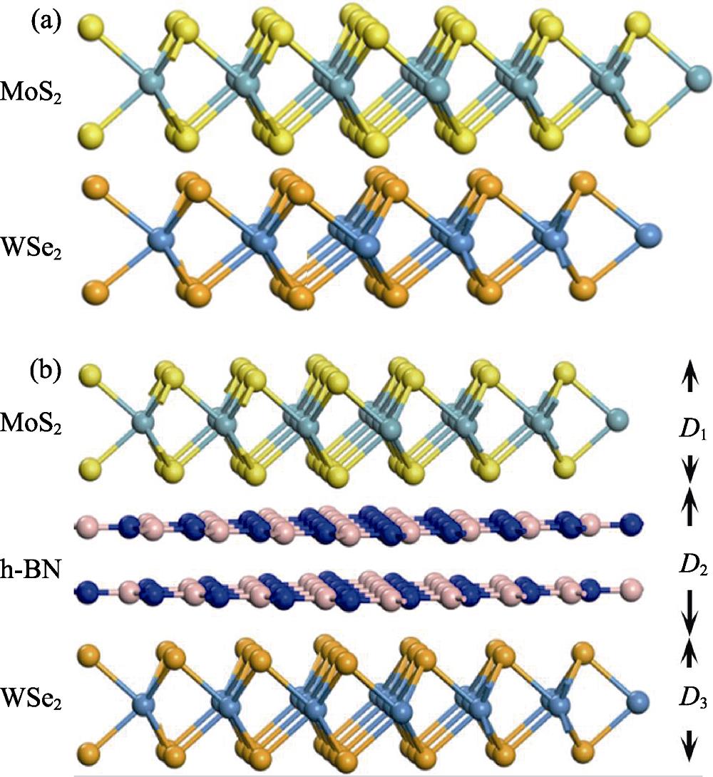
[9] S LATINI, T WINTHER K, T OLSEN et al. Interlayer excitons and band alignment in MoS2/h-BN/WSe2 van der Waals heterostructures. Nano Lett., 17, 938-945(2017).
[10] Y KIM J, G KIM S, W YOUN J et al. Energy and charge transfer effects in two-dimensional van der Waals hybrid nanostructures on periodic gold nanopost array. Appl. Phys. Lett., 112, 193101(2018).
[11] L YANG, X YU, M XU et al. Interface engineering for efficient and stable chemical-doping-free graphene-on-silicon solar cells by introducing a graphene oxide interlayer. J. Mater. Chem. A, 2, 16877-16883(2014).
[12] H MENG J, X LIU, W ZHANG X et al. Interface engineering for highly efficient graphene-on-silicon Schottky junction solar cells by introducing a hexagonal boron nitride interlayer. Nano Energy, 28, 44-50(2016).
[13] F SUN W, C LI M, C ZHAO L. First-principles investigation of carrier Auger lifetime and impact ionization rate in narrow-gap superlattices. Acta Phys. Sin., 59, 5661-5666(2010).
[14] Y HE, G OUYANG. Geometry-dependent Auger recombination process in semiconductor nanostructures. J. Phys. Chem. C, 121, 23811-23816(2017).
[16] Q LI, T LIAN. Area- and thickness-dependent biexciton Auger recombination in colloidal CdSe nanoplatelets: breaking the “universal volume scaling law”. Nano Lett., 17, 3152-3158(2017).
[17] D LIU S, T CHENG M, J ZHOU H et al. The effect of biexciton, wetting layer leakage and Auger capture on Rabi oscillation damping in quantum dots. Acta Phys. Sin., 55, 2122-2127(2006).
[18] M DENNIS A, D MANGUM B, A PIRYATINSKI et al. Suppressed blinking and Auger recombination in near-infrared type-II InP/CdS nanocrystal quantum dots. Nano Lett., 12, 5545-5551(2012).
[19] S PARK Y, K BAE W, A PADILHA L et al. Effect of the core/shell interface on Auger recombination evaluated by single-quantum-dot spectroscopy. Nano Lett., 14, 396-402(2014).
[21] R VAXENBURG, A RODINA, E LIFSHITZ et al. Biexciton Auger recombination in CdSe/CdS core/shell semiconductor nanocrystals. Nano Lett., 16, 2503-2511(2016).
[23] R BEATTIE A, T LANDSBERG P. Auger effect in semiconductors. Proc. R. Soc. London. Ser. A, 249, 16-29(1959).
[27] A ZHANG, Z ZHU, Y HE et al. Structure stabilities and transitions in polyhedral metal nanocrystals: an atomic-bond-relaxation approach. Appl. Phys. Lett., 100, 171912(2012).
[28] Z ZHU, A ZHANG, G OUYANG et al. Edge effect on band gap shift in Si nanowires with polygonal cross-sections. Appl. Phys. Lett., 98, 263112(2011).
[35] T KIRCHARTZ, J MATTHEIS, U RAU. Detailed balance theory of excitonic and bulk heterojunction solar cells. Phys. Rev. B, 78, 235320(2008).
[40] J WANG, F MA, W LIANG et al. Optical, photonic and optoelectronic properties of graphene, h-BN and their hybrid materials. Nanophotonics, 6, 943-976(2017).
[43] S CHOI M, H LEE G, J YU Y et al. Controlled charge trapping by molybdenum disulphide and graphene in ultrathin heterostructured memory devices. Nat. Commun., 4, 1624(2013).
[44] S YUN W, W HAN S, C HONG S et al. Thickness and strain effects on electronic structures of transition metal dichalcogenides: 2H-MX2 semiconductors (M=Mo, W; X=S, Se, Te). Phys. Rev. B, 85, 033305(2012).
[45] F GARCÍA-SANTAMARÍA, S BROVELLI, R VISWANATHA et al. Breakdown of volume scaling in Auger recombination in CdSe/CdS heteronanocrystals: the role of the core-shell interface. Nano Lett., 11, 687-693(2011).