Abstract
Realization of efficient yellow-light-emitting diodes (LEDs) has always been a challenge in solid-state lighting. Great effort has been made, but only slight advancements have occurred in the past few decades. After comprehensive work on InGaN-based yellow LEDs on Si substrate, we successfully made a breakthrough and pushed the wall-plug efficiency of 565-nm-yellow LEDs to 24.3% at and 33.7% at . The success of yellow LEDs can be credited to the improved material quality and reduced compressive strain of InGaN quantum wells by a prestrained layer and substrate, as well as enhanced hole injection by a 3D pn junction with V-pits.1. INTRODUCTION
Since the first practical visible-spectrum light-emitting diode (LED) was invented in 1962 [1], great achievements have been made in solid-state lighting in the past half century. LEDs in the entire visible light range were successfully developed, providing us with a colorful artificial-vision world. However, LEDs are not maturely developed currently. Blue and red LEDs are very efficient with external quantum efficiency (EQE) above 80% [2] and 50% [3], respectively, whereas yellow LEDs are inefficient, which is known as the “green gap” but precisely should be called the “yellow gap.” That is why professor Holonyak, the inventor of the red LED, said in 2012, “LED is in its infancy; nobody has solved the problem of getting yellow LED very well.”
A lack of efficient yellow LEDs leads to phosphor conversion of blue LEDs for white lighting, the efficiency of which is much higher than that of incandescent and fluorescent lamps, but there is still great room for power efficiency and spectrum quality improvement. Mixing multi-color LEDs to form white light provides a promising way to attain the balance among the color rendering index (CRI), correlated color temperature (CCT), and light efficiency, which is a basis of smart lighting. Meanwhile, the blue light hazard is attracting great attention, which can also be minimized by color mixing (CM) LEDs if the spectra are properly designed. Also, CM-LEDs can be applied in the new technology of visible light communication, rather better than phosphor-converted LEDs, as there is no response delay raised by the phosphor. Obviously, CM-LEDs have a very bright future. Since blue, green, and red LEDs are already commercially available with high efficiency, all we need to do is to make yellow LEDs efficient.
For many decades, the wall-plug efficiencies (WPEs) of direct yellow LEDs have been lower than 10% [4]. In 1971, Craford et al. [5] fabricated the first yellow LED using nitrogen-doped GaAsP with a WPE of about 0.01%. In the 1990s, the HP Company developed the AlGaInP-based yellow LEDs with double-hetero structure [6,7], and the WPE was improved to 1.3%. In 2008, Satoa et al. [8] prepared InGaN-based yellow LEDs on semi-polar GaN substrate with the purpose of reducing the piezoelectric field in InGaN quantum wells (QWs). The WPE was pushed to 5.4%, even if the EQE was increased to 13.4%, but the voltage was as high as 5.4 V. In 2013, the Toshiba Company reported its InGaN-based yellow LEDs grown on -faced sapphire substrate [9], with the key technology of inserting an AlGaN interlayer between the InGaN well and GaN barrier. The EQE was increased to 18.9%, but again the voltage was as high as 4.34 V, and thus finally, the WPE was only 9.4%. In 2014, high-power yellow LEDs on silicon substrate were first fabricated by our group, with 74 mW light output power and 9.4% EQE at 350 mA driving current [10].
Sign up for Photonics Research TOC. Get the latest issue of Photonics Research delivered right to you!Sign up now
Neither the InGaN nor AlGaInP system performs well in the yellow emission region. A physical bottleneck restricts the AlGaInP system as the bandgap transits from direct to indirect when wavelength shifts from red to yellow, while the challenge for the InGaN system is in material growth. In general, the relatively lower efficiency for the long wavelength of the InGaN system can be attributed mainly to its high indium content. To incorporate more indium, low temperature is required to grow the InGaN QWs, which restrains the cracking efficiency of ammonia and reduces the diffusion ability of surface atoms, resulting in a coarse interface, high dislocation density, and high point defect density. Also, limited solubility of InN in GaN may cause phase separation in the QWs. Moreover, a high piezoelectric effect existing in InGaN wells leads to a quantum Stark effect and causes carrier separation and electron overflow from the active region. All these are unfavorable for the efficiency of yellow LEDs. In this work, integrated works have been done to explore the potential of InGaN in yellow light emission, and preliminary achievements have been made.
2. METHODS AND RESULTS
The material growth was carried out by a homemade metal–organic chemical vapor deposition (MOCVD) reactor with a specially designed vertical close-coupled co-axis showerhead [11]. A patterned Si (111) wafer was selected as the substrate [12]. The large lattice and thermal mismatch between Si and GaN create great challenges in material growth, but also bring the opportunity to grow high-quality InGaN QWs with high indium content. Once dislocation density and film cracking are under control, the tensile-type thermal strain and lattice strain raised by the Si substrate become positive factors for indium incorporation. Growth temperature can be enhanced to improve the quality of QWs.
As illustrated in Fig. 1, epitaxy started from a 100-nm high temperature (HT) AlN buffer, and then three-dimensional GaN islands were grown on the AlN buffer with the assistance of lattice strain between GaN and AlN, followed by a GaN recovery layer to coalesce the separated islands. After that, n-GaN was grown with a thickness of 3 μm and Si doping of .
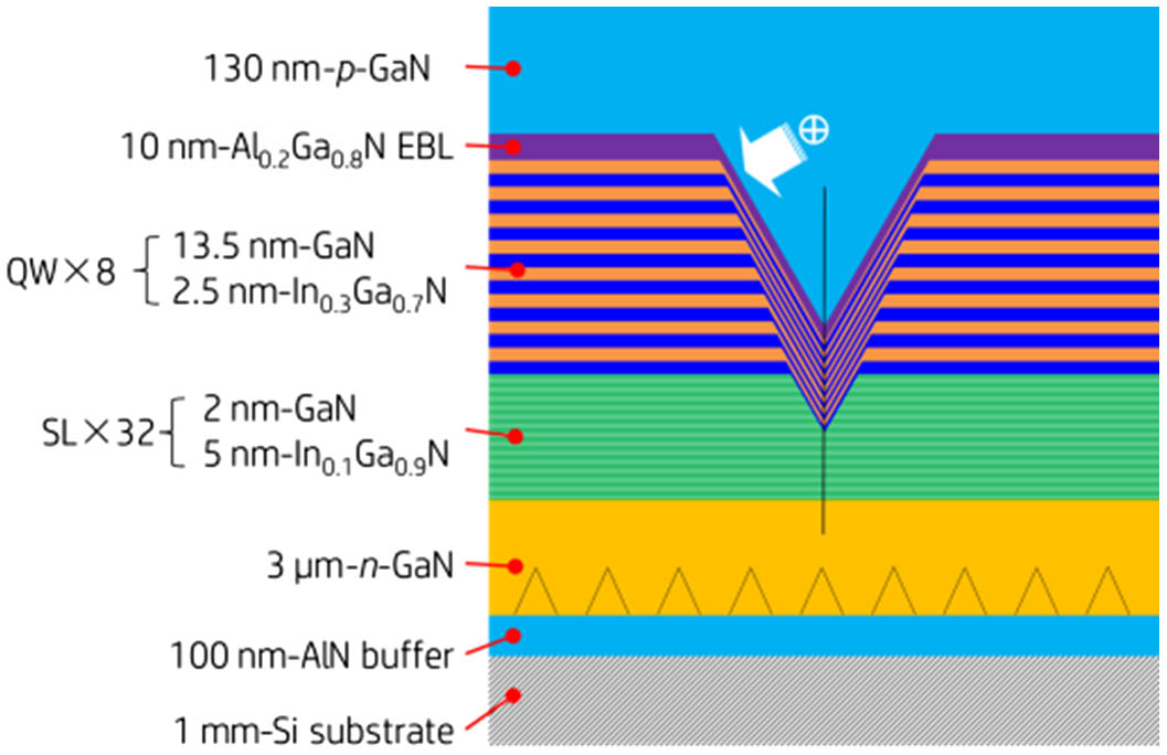
Figure 1.Schematic epitaxial structure of an InGaN yellow LED grown on Si substrate.
Prior to the QWs, 32 periods of 5-nm-In0.1Ga0.9N/2-nm-GaN superlattice (SL) interlayers were grown, which was to release the strain in the QWs and generate V-pits at the dislocation sites. The interlayers with optimized indium content not only help strain evolve more gently from n-GaN to InGaN QWs, but also maintain the crystal quality at a high level.
For InGaN on Si substrate, V-pits can initialize at each site of dislocations under special conditions, such as low growth temperature and nitrogen ambience. A transmission electron microscope (TEM) image of a V-pit in the active region of the yellow LED is shown in Fig. 2(a). The V-pits were reported to have thinner QWs at the sidewalls, which is helpful to screen the dislocations and enhance radiative recombination efficiency [13]. More than that, we suggest a new concept of a “3D pn junction” with a V-pit structure. Unlike traditional diodes with a planar boundary between the p-side and the n-side, the existence of V-pits forms a cross-connected boundary between the p-side and the n-side, as shown in Fig. 2(b). Carrier transportation of an LED with V-pits is totally different from that of planar pn junction, which should be considered three dimensionally. Simulation and experimental results show that V-pits can help to enhance hole injection from V-pit sidewalls [14–18], as the effective barrier from the sidewall of V-pits is lower than that from the flat multiple quantum wells (MQWs) for holes.

Figure 2.(a) TEM image of a V-pit and (b) schematic 3D pn junction with V-pit structure.
The QWs consisted of eight periods of InGaN/GaN with four steps in each period. Temperature was first ramped down to 780°C to grow a 0.5-nm-thick GaN prelayer with the purpose of repairing the surface damaged during the temperature ramping process. Then the well was grown with an optimized thickness of 2.5 nm, and covered by a 2-nm-thick GaN protective cap before the temperature was ramped up to 950°C to grow an 11-nm-thick HT GaN barrier. The first seven barriers were slightly doped with Si to reduce forward voltage, and the last barrier was undoped. A 10-nm-thick electron blocking layer (EBL) with Mg doping was grown after the QWs, followed by a 50-nm-thick p-GaN layer with Mg doping for hole injection, then a V-pit recovery layer was grown to fill up the V-pits, and finally the structure ended with a 20-nm-thick highly Mg-doped () p-contact layer for making p-contact.
Images of fluorescent luminescence (FL) spectrometry (Nikon C-HGFI) excited by 500–530 nm intensive light are presented in Fig. 3. Pure yellow light with homogenous InGaN phase could be observed, which reveals fine MQW quality.
Figure 3.FL morphology of InGaN QWs of a yellow LED on Si substrate.
The LED structure was scanned by a high-resolution X-ray diffractor (Pan Analytic X’Pert). As shown in Fig. 4, satellite peaks of QWs from up to can be clearly observed; six secondary-order satellite peaks between QWs-1 and QWs-0 can also be differentiated, indicating very abrupt interfaces within the QW structure. The diffraction peaks of SLs are also very sharp, indicating the fine quality of the prestrained interlayers.
Figure 4.Omega-2theta scan curve of the yellow InGaN LED structure grown on Si substrate.
Second ion mass spectra (SIMS) measurement was carried out by CAMECA IMS-7F from the top surface of p-GaN to verify the depth and doping profiles of the LED structure. As shown in Fig. 5, the Si doping concentrations are and in n-GaN and the barrier, respectively. The Mg doping concentrations are and in the hole injection layer and p-contact layer, respectively. Note that the elements of Mg and Al penetrate through the QW region into the SL interlayers, which is not due to the presence of the pushing effect by primary ions of SIMS, but is caused by the filling of Mg and Al into the V-pits when V-pits were opened during growth procedures. The penetration depth, around 150 nm, is possible corresponding to the depth of V-pits when finishing the growth of QWs. The clear oscillation of the indium profile again reveals abrupt interfaces of QWs and SLs.
Figure 5.SIMS depth profile of Mg-In-Al-Si in the yellow LED structure on Si substrate.
The as-grown epitaxial film was fabricated into vertical thin film LEDs with the top surface roughened and the backside coated with an Ag-reflector via a film transferring technique [19], with a size of . Electroluminescence properties of the devices were tested under continuous-wave (CW) mode by Keithley Instruments 2635A as the source meter and Instrument Systems CAS140CT as the spectrometer. The latest results of WPE accomplished with light output power (LOP) are plotted as functions of current density in Fig. 6. The WPE curve of the yellow LED shows similar droop behavior as InGaN-based blue and green LEDs; it increases sharply and then droops slowly with the current density. At , WPE reaches its peak, where the value is 33.7%, and the corresponding dominant wavelength (WLD), LOP, and forward voltage (Vf) are 574 nm, 21.2 mW, and 2.10 V, respectively. The EQE is 32.7%, and luminous efficacy reaches 192 lm/W. Note that the average energy of emitted photons (2.16 eV) is larger than the potential drop in voltage (2.10 eV); the extra energy may come from the thermal energy () carried by carriers. Increasing current density to , WPE drops down to 24.3%, where the WLD, LOP, and Vf are 565 nm, 116 mW, and 2.39 V, respectively. The EQE is 26.4% and luminous efficacy reaches 149 lm/W. The efficiency droop from peak to is calculated to be 28%, whereas the values are around 10% and 20% for blue and green LEDs, respectively. The severer efficiency droop for yellow LEDs could be attributed to the stronger piezoelectric field existing in the QWs.
Figure 6.Plot of WPE and light output power as functions of current density for a yellow LED on Si substrate.
The above data of the 565-nm yellow LED are the latest results of our group. Before that, a series of InGaN-based LEDs with various wavelengths ranging from green to orange was successfully developed on Si substrate. The characterizations of WPE, voltage, and full width at half maxima (FWHM) depending on wavelength are plotted in Fig. 7. All the devices are , measured under CW mode at 200 mA (). The WPE of the InGaN LEDs is 41.3% at 522 nm and 11.6% at 585 nm, which decreases approximately linearly with increasing wavelength. Fitting the data linearly shows that WPE decays 0.47% per nanometer. Counting in eye sensitivity function (ESF), the luminous efficacy exhibits a different trend compared with WPE. It has a peak value of 193 lm/W at 528 nm, and drops down slowly to 165 lm/W until ESF reaches its maxima at 555 nm, and then drops down rapidly to 55 lm/W, as both WPE and ESF decrease. The voltage of the devices shows a negative relationship with wavelength, which follows the nature that bandgap energy decreases with increasing wavelength. The FWHM is found to be narrow for short wavelengths and broad for long wavelengths; this could be attributed to the indium fluctuation and piezoelectric effect within the QWs. More indium content leads to severer indium fluctuation and a stronger piezoelectric field.
Figure 7.Dependence of (a) WPE, (b) efficacy, (c) voltage, and (d) FWHM on wavelength for InGaN-based LEDs on Si substrate from the green to orange emission range.
CM white LEDs made by mixing InGaN-based blue, cyan, green, and yellow LEDs on silicon substrate, together with AlGaInP red LEDs, are successfully developed and commercialized. The spectrum of a CM-LED module measured at under CW mode is presented in Fig. 8. With color coordinates (, ) lying right on Planckian locus, the sample () gets a high CRI (Ra: 97.5 and R9: 96.2) and a high efficacy of 121.3 lm/W, which is comparable with those PC-LEDs with similar CCT and CRI.
Figure 8.Spectrum of a CM white LED without phosphor made up by InGaN blue, cyan, green, and yellow LEDs and AlGaInP red LEDs.
3. CONCLUSION
In conclusion, we made a significant breakthrough in the “yellow gap” by improving the quality of InGaN, reducing the strain in QWs, and utilizing the 3D pn junction of V-pits. Efficient InGaN-based yellow LEDs on Si substrate have been fabricated. A record-high WPE of 24.3% with 149 lm/W at was obtained for a 565-nm yellow LED, and the WPE peak reaches 33.7% with 192 lm/W at . A CM white LED made by InGaN blue, cyan, green, and yellow LEDs and AlGaInP red LEDs was demonstrated with Ra as high as 97.5, luminous efficacy above 120 lm/W, and CCT of 2941 K. The efficient yellow LED promotes development of next-generation solid state lighting without phosphor, and will be shining in various application areas such as general lighting, smart lighting, and visible light communication.
References
[1] N. Holonyak, S. F. Bevacqua. Coherent (visible) light emission from Ga(As1-xPx) junctions. Appl. Phys. Lett., 1, 82-83(1962).
[2] Y. Narukawa, M. Ichikawa, D. Sanga, M. Sano, T. Mukai. White light emitting diodes with super-high luminous efficacy. J. Phys. D, 43, 354002(2010).
[3] M. R. Krames, H. M. Ochiai, G. E. Hofler, C. C. Carter. High-power truncated inverted pyramid (AlxGa1-x)0.5In0.5P/GaP light-emitting diodes exhibiting >50% external quantum efficiency. Appl. Phys. Lett., 75, 2365-2367(1999).
[4] B. Damilano, B. Gil. Yellow-red emission from (Ga,In)N heterostructures. J. Phys. D, 48, 403001(2015).
[5] W. O. Groves, A. H. Herzog, M. G. Craford. The effect of nitrogen doping on GaAs1-xPx electroluminescent diodes. Appl. Phys. Lett., 19, 184-186(1971).
[6] C. P. Kuo, R. M. Fletcher, T. D. Osentowski, M. C. Lardizabal, M. G. Craford, V. M. Robbins. High performance AlGaInP visible light-emitting diodes. Appl. Phys. Lett., 57, 2937-2939(1990).
[7] F. A. Kish, F. M. Steranka, D. C. DeFevere, D. A. Vanderwater, K. G. Park, C. P. Kuo, T. D. Osentowski, M. J. Peanasky, J. G. Yu, R. M. Fletcher, D. A. Steigerwald, M. G. Craford. Very high-efficiency semiconductor wafer-bonded transparent-substrate (AlxGa1-x)0.5In0.5P/GaP light-emitting diodes. Appl. Phys. Lett., 64, 2839-2841(1994).
[8] H. Satoa, R. B. Chung, H. Hirasawa, N. Fellows, H. Masui, F. Wu, M. Saito, K. Fujitob, J. S. Speck, S. P. DenBaars, S. Nakamura. Optical properties of yellow light-emitting diodes grown on semipolar (11-22) bulk GaN substrates. Appl. Phys. Lett., 92, 221110(2008).
[9] S. Saito, R. Hashimoto, J. Hwang, S. Nunoue. InGaN light-emitting diodes on c-face sapphire substrates in green gap spectral range. Appl. Phys. Express, 6, 111004(2013).
[10] J. Zhang, C. Xiong, J. Liu, Z. Quan, L. Wang, F. Jiang. High brightness InGaN-based yellow light-emitting diodes with strain modulation layers grown on Si substrate. Appl. Phys. A, 114, 1049-1053(2014).
[11] F. Jiang, Y. Pu. Double inlet showerhead for metal organic vapor deposition reactor. CN patent(2006).
[12] J. Liu, J. Zhang, Q. Mao, X. Wu, F. Jiang. Effects of AlN interlayer on growth of GaN-based LED on patterned silicon substrate. CrystEngComm, 15, 3372-3376(2013).
[13] A. Hangleiter, F. Hitzel, C. Netzel, D. Fuhrmann, U. Rossow, G. Ade, P. Hinze. Suppression of nonradiative recombination by V-shaped pits in GaInN/GaN quantum wells produces a large increase in the light emission efficiency. Phys. Rev. Lett., 95, 127402(2005).
[14] X. Wu, J. Liu, Z. Quan, C. Xiong, C. Zheng, J. Zhang, Q. Mao, F. Jiang. Electroluminescence from the sidewall quantum wells in the V-shaped pits of InGaN light emitting diodes. Appl. Phys. Lett., 104, 221101(2014).
[15] Z. Quan, L. Wang, C. Zheng, J. Liu, F. Jiang. Roles of V-shaped pits on the improvement of quantum efficiency in InGaN/GaN multiple quantum well light-emitting diodes. J. Appl. Phys., 116, 183107(2014).
[16] X. Wu, J. Liu, F. Jiang. Hole injection from the sidewall of V-shaped pits into c-plane multiple quantum wells in InGaN light emitting diodes. J. Appl. Phys., 118, 164504(2015).
[17] Z. Quan, J. Liu, F. Fang, G. Wang, F. Jiang. A new interpretation for performance improvement of high-efficiency vertical blue light-emitting diodes by InGaN/GaN superlattices. J. Appl. Phys., 118, 193102(2015).
[18] C. Li, C. Wu, C. Hsu, L. Lu, H. Li, T. Lu, Y. Wu. 3D numerical modeling of the carrier transport and radiative efficiency for InGaN/GaN light emitting diodes with V-shaped pits. AIP Adv., 6, 055208(2016).
[19] J. Liu, J. Zhang, G. Wang, C. Mo, L. Quan, J. Din, Z. Quan, X. Wang, S. Pan, C. Zheng, X. Wu, W. Fang, F. Jiang. Status of GaN-based green light-emitting diodes. Chin. Phys. B, 24, 067804(2015).


