• Photonics Research
  • Vol. 10, Issue 7, 1533 (2022)
Meng Li1、2、†, Chu Li1、2、†, Yang Chen3, Lan-Tian Feng3, Linyu Yan1、2, Qian Zhang1、2, Jueming Bao1、2, Bi-Heng Liu3, Xi-Feng Ren3、6、*, Jianwei Wang1、2、4、5, Shufeng Wang1、2、4、5, Yunan Gao1、2、4、5, Xiaoyong Hu1、2、4、5, Qihuang Gong1、2、4、5, and Yan Li1、2、4、5、7、*
Author Affiliations
  • 1State Key Laboratory for Artificial Microstructure and Mesoscopic Physics, School of Physics, Peking University, Beijing 100871, China
  • 2Frontiers Science Center for Nano-Optoelectronics, Peking University, Beijing 100871, China
  • 3Key Laboratory of Quantum Information, CAS University of Science and Technology of China, Hefei 230026, China
  • 4Collaborative Innovation Center of Extreme Optics, Shanxi University, Taiyuan 030006, China
  • 5Peking University Yangtze Delta Institute of Optoelectronics, Nantong 226010, China
  • 6e-mail: renxf@ustc.edu.cn
  • 7e-mail: li@pku.edu.cn
  • show less
    DOI: 10.1364/PRJ.452539 Cite this Article Set citation alerts
    Meng Li, Chu Li, Yang Chen, Lan-Tian Feng, Linyu Yan, Qian Zhang, Jueming Bao, Bi-Heng Liu, Xi-Feng Ren, Jianwei Wang, Shufeng Wang, Yunan Gao, Xiaoyong Hu, Qihuang Gong, Yan Li. On-chip path encoded photonic quantum Toffoli gate[J]. Photonics Research, 2022, 10(7): 1533 Copy Citation Text show less
    Circuit design of the Toffoli gate. (a) Schematic of the 3D layout of the path encoded three-qubit Toffoli gate for FLDW. The 3D quantum circuit is adapted from the 2D theoretical work in Ref. [48], where the blue, red, and green curves correspond to the top-path, bottom-path, and depth-varying overpass waveguides, respectively. There are 10 DCs in this circuit, and the number marked on each DC stands for reflectivity R. DCs (2), (3), and (4) construct a local classical interferometer. Two parts (yellow curves) marked Δ stand for path compensation for the global unsymmetrical MZ interferometer. The depth change of the overpass waveguide is 20 μm. Two magenta boxes marked φ represent additional phase shifts (−π/2) that should be compensated at the input and output ports. (b) The CAD layout of the Toffoli gate. (c) Micrograph of the DC with the reflectivity of 1/3 and the enlarged view of the coupling region. (d) Micrograph of the waveguides in different depths without crossing.
    Fig. 1. Circuit design of the Toffoli gate. (a) Schematic of the 3D layout of the path encoded three-qubit Toffoli gate for FLDW. The 3D quantum circuit is adapted from the 2D theoretical work in Ref. [48], where the blue, red, and green curves correspond to the top-path, bottom-path, and depth-varying overpass waveguides, respectively. There are 10 DCs in this circuit, and the number marked on each DC stands for reflectivity R. DCs (2), (3), and (4) construct a local classical interferometer. Two parts (yellow curves) marked Δ stand for path compensation for the global unsymmetrical MZ interferometer. The depth change of the overpass waveguide is 20 μm. Two magenta boxes marked φ represent additional phase shifts (π/2) that should be compensated at the input and output ports. (b) The CAD layout of the Toffoli gate. (c) Micrograph of the DC with the reflectivity of 1/3 and the enlarged view of the coupling region. (d) Micrograph of the waveguides in different depths without crossing.
    Two-photon quantum interference curves. Coincidence counts of post-selected output two-photon combinations (i′, j′) denoted as Ci′j′ for different input two-photon combinations (i, j) denoted as Input (i, j) as a function of the relative delay of photons’ input in the i and j ports: (a) input (5, 2); (b) input (5, 3); (c) input (6, 2); (d) input (6, 3). From the interference curves with a deep dip, the HOM interference visibilities are (a) 86.5%±2.8%, (b) 89.5%±2.5%, (c) 98.8%±0.9%, and (d) 98.3%±0.9%, respectively. The error bars are all calculated by assuming Poisson statistics. The insets demonstrate the main evolution of two photons in the chip. The pairs of filled circles are coincident photons, and the pairs of the hollow circles represent the disappearance of coincident photons due to the quantum interferences.
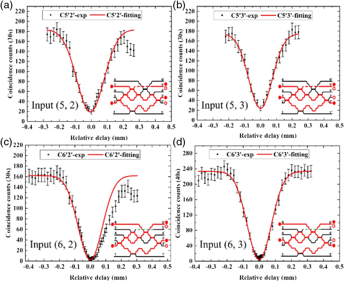
    Fig. 2. Two-photon quantum interference curves. Coincidence counts of post-selected output two-photon combinations (i, j) denoted as Cij for different input two-photon combinations (i, j) denoted as Input (i, j) as a function of the relative delay of photons’ input in the i and j ports: (a) input (5, 2); (b) input (5, 3); (c) input (6, 2); (d) input (6, 3). From the interference curves with a deep dip, the HOM interference visibilities are (a) 86.5%±2.8%, (b) 89.5%±2.5%, (c) 98.8%±0.9%, and (d) 98.3%±0.9%, respectively. The error bars are all calculated by assuming Poisson statistics. The insets demonstrate the main evolution of two photons in the chip. The pairs of filled circles are coincident photons, and the pairs of the hollow circles represent the disappearance of coincident photons due to the quantum interferences.
    Schematic of the quantum characterization system. (a) The 808 nm femtosecond laser pulses pass through a frequency-doubling crystal (BBO1) to generate linearly polarized 404 nm ultraviolet pulses, and the ultraviolet pulses are focused on two cascaded beamlike II BBO crystals (BBO2&BBO3) to produce two pairs of photons with quantum correlation. The photons are injected into chips and collected to make four-fold coincidence measurement. M, mirror; DM, dichroic mirror; HWP, half-wave plate; SPF, short-pass filter (<650 nm); IF, interference filters at 808 nm; GTP, Glan–Taylor polarizer; L, lens; BBO, β–BaB2O4 crystal; P, prism; CL, coupling lens; SPCMs, single-photon counting modules; FA, fiber array; DL, delay line; TDC, time-to-digital converter. (b) Two-photon quantum interference curve of the dependent photons 1&2 on a balanced FBS (V=94.7%±0.2%). (c) Four-photon quantum interference curve of the independent photons 2&3 on a balanced FBS (V=83.1%±3.2%). The error bars are all calculated by assuming Poisson statistics.
    Fig. 3. Schematic of the quantum characterization system. (a) The 808 nm femtosecond laser pulses pass through a frequency-doubling crystal (BBO1) to generate linearly polarized 404 nm ultraviolet pulses, and the ultraviolet pulses are focused on two cascaded beamlike II BBO crystals (BBO2&BBO3) to produce two pairs of photons with quantum correlation. The photons are injected into chips and collected to make four-fold coincidence measurement. M, mirror; DM, dichroic mirror; HWP, half-wave plate; SPF, short-pass filter (<650  nm); IF, interference filters at 808 nm; GTP, Glan–Taylor polarizer; L, lens; BBO, βBaB2O4 crystal; P, prism; CL, coupling lens; SPCMs, single-photon counting modules; FA, fiber array; DL, delay line; TDC, time-to-digital converter. (b) Two-photon quantum interference curve of the dependent photons 1&2 on a balanced FBS (V=94.7%±0.2%). (c) Four-photon quantum interference curve of the independent photons 2&3 on a balanced FBS (V=83.1%±3.2%). The error bars are all calculated by assuming Poisson statistics.
    Truth table of the path encoded three-qubit Toffoli gate at computation basis. The filled bars are the normalized experimental reconstructed data, and the unfilled ones are the ideal values. The average fidelity of the truth table of this Toffoli gate is 85.5%±0.6%.
    Fig. 4. Truth table of the path encoded three-qubit Toffoli gate at computation basis. The filled bars are the normalized experimental reconstructed data, and the unfilled ones are the ideal values. The average fidelity of the truth table of this Toffoli gate is 85.5%±0.6%.
    Schematic of the 3D layout of the path encoded four-qubit CCCNOT gate for FLDW and the experimental characterization with classical light. (a) The green and light green curves correspond to depth-varying overpass waveguides, and the red curve stands for the waveguides deformed to generate a phase shift Δϕ=π. Two parts marked Δ correspond to path compensation for the global MZ interferometer, and two magenta boxes marked φ represent additional phase shifts (−π/2) that should be compensated at the input and output ports. (b) Theoretical output power distribution for each single port input. (c) Experimental output power distribution for each single port input when the injected laser is centered at 808 nm with V polarization. The similarity (S) of the output power distribution for this CCCNOT gate is 99.2%±0.8%.
    Fig. 5. Schematic of the 3D layout of the path encoded four-qubit CCCNOT gate for FLDW and the experimental characterization with classical light. (a) The green and light green curves correspond to depth-varying overpass waveguides, and the red curve stands for the waveguides deformed to generate a phase shift Δϕ=π. Two parts marked Δ correspond to path compensation for the global MZ interferometer, and two magenta boxes marked φ represent additional phase shifts (π/2) that should be compensated at the input and output ports. (b) Theoretical output power distribution for each single port input. (c) Experimental output power distribution for each single port input when the injected laser is centered at 808 nm with V polarization. The similarity (S) of the output power distribution for this CCCNOT gate is 99.2%±0.8%.
    Experimental characterization of a typical Toffoli gate with classical light. (a) Theoretical output power distribution for each input port. (b) Experimental output power distribution for each single input port when the injected laser is centered at 808 nm with V polarization. The similarity (S) of the output power distribution for this Toffoli gate is 98.2%±1.7%.
    Fig. 6. Experimental characterization of a typical Toffoli gate with classical light. (a) Theoretical output power distribution for each input port. (b) Experimental output power distribution for each single input port when the injected laser is centered at 808 nm with V polarization. The similarity (S) of the output power distribution for this Toffoli gate is 98.2%±1.7%.
    Meng Li, Chu Li, Yang Chen, Lan-Tian Feng, Linyu Yan, Qian Zhang, Jueming Bao, Bi-Heng Liu, Xi-Feng Ren, Jianwei Wang, Shufeng Wang, Yunan Gao, Xiaoyong Hu, Qihuang Gong, Yan Li. On-chip path encoded photonic quantum Toffoli gate[J]. Photonics Research, 2022, 10(7): 1533
    Download Citation