Author Affiliations
1Department of Chemistry, Universidad Técnica Particular de Loja, 110160 Loja, Ecuador2UNICARIBE Research Center, University of Calabria, I-87036 Rende, CS, Italy3Grupo de Investigación en Materiales Avanzados (GIMA), Facultad de Ciencias, Escuela Superior Politécnica de Chimborazo (ESPOCH), Riobamba, Ecuador4Facultad de Ciencias, Escuela Superior Politécnica de Chimborazo (ESPOCH), Riobamba, Ecuador5Faculty of Mechanical Engineering, Escuela Superior Politécnica de Chimborazo (ESPOCH), Riobamba 060155, Ecuador6INFN-Laboratori Nazionali di Frascati, Via E. Fermi 54, I-00044 Frascati, Italyshow less
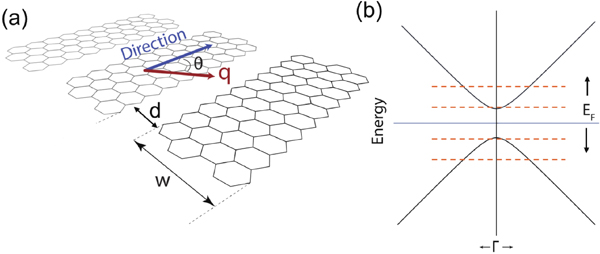
Fig. 1. (Color online) (a) Schematic representation of GeNSs. (b) Hypothetical low-energy band structure of GeNSs, showing the modulation of charge carrier density by shifting the Fermi level (orange dashed lines).
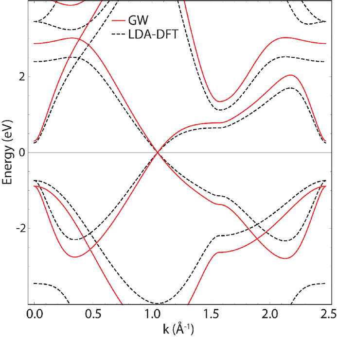
Fig. 2. (Color online) Full-electron band structure of freestanding germanene along the path by using the approach of the GW approximation (continues red) and conventional DFT (dashed black) computations.
Fig. 3. (Color online) (a) Low-energy band structure of freestanding germanene in the vicinity of the Fermi level and K-point. The energy bands and resemble green and black, respectively. The linear fit is indicated by the cyan line. (b) Color plot depicting the group velocity of suspended germanene near the K point. The plot shows how the carrier velocity changes with energy and wavevector. The group velocity with negative values is the carrier velocity in the valence band.
Fig. 4. (Color online) Variation of bandgap in (a) narrow GeNSs (10−50 nm wide) and (b) wide GeNSs (100−500 nm wide). The estimated bandgaps via GW-group velocity are compared with those values via DFT-group velocity.
Fig. 5. (Color online) Electron band structure and DOS of GeNSs with widths of (a), (b) 100 nm and (c), (d) 500 nm. The smoothed curve of the histogram is shown by the red line.
Fig. 6. (Color online) The system under study corresponds to a 100 nm wide nanostrip (, = 0°, ). (a) Dispersion of the plasmon frequency-momentum as a function of the wave vector, considering different values of . (b) Plasmon spectra for selected values of momenta. (c) Density plot of the dispersion of the plasmon frequency as a function of carrier density versus wave vector.
Fig. 7. (Color online) (a) Dispersion of the plasmon frequency-momentum as a function of the wave vector, considering different values of ) (see Table 2). The extra modeling parameters are = 0°, cm−2, and . (b) Plasmon spectra at cm−1 for different values of ). (c) Density plot of the dispersion of the plasmon frequency as a function of effective electron masses versus wave vector.
Fig. 8. (Color online) (a) Dispersion of the plasmon frequency-momentum as a function of the wave vector, considering different values of . The current system corresponds to a 100 nm wide strip with fixed parameters as: cm−2, , and . (b) Plasmon spectra at cm−1 for selected values of . (c) Density plot of the dispersion of the plasmon frequency as a function of excitation angles versus wave vector.
Fig. 9. (Color online) (a) Dispersion of the plasmon frequency-momentum as a function of the wave vector (, cm−1), considering different values of electron relaxation rate. (b) Maximum of the plasmon peak at cm−1 for selected values of electron relaxation rate. (c) Density plot of plasmon frequency-momentum dispersion as a function of electron relaxation rate and wave vector. The analyzed system corresponds to a 100 nm wide nanostrip ( cm−2, , = 0°).
Method | Value (106 m·s−1) | Variation percentage (%) |
---|
LDA-DFT | 0.527 | −24.93 | GW | 0.702 | −37.21 | GW-gr | 1.118 | +1.64 | Exp-gr | 1.1 | − |
|
Table 0. The estimated group velocity of suspended germanene and graphene by GW and DFT calculations compared with the available experimental value.
(1013 s−1) | (1012 s−1) | mobility (cm2/(V∙s)) |
---|
0.5 | 2.5 | 57705 | 1.0 | 5.0 | 48677 | 1.5 | 7.5 | 39650 | 2.0 | 10 | 30622 |
|
Table 0. Estimated values of electron relaxation rate (), plasmon relaxation rate (), and electron mobility ().
(nm) | (cm−2) | (eV) |
---|
10 | | 0.37 | 20 | | 0.26 | 50 | | 0.16 | 100 | | 0.12 |
|
Table 0. Variation of carrier density and Fermi level by adjusting the distance between GeNSs.
Strip width (nm) | (meV) | (10−3) |
---|
100 | 29.03 | 5.18 | 200 | 14.52 | 2.59 | 300 | 9.68 | 1.73 | 400 | 7.26 | 1.30 | 500 | 5.81 | 1.04 |
|
Table 0. Bandgap values and effective electron masses of chosen GeNSs (see Fig. 3(b)). It is pointed out that denotes the free electron mass.