Germanene nanostrips (GeNSs) have garnered significant attention in modern semiconductor technology due to their exceptional physical characteristics, positioning them as promising candidates for a wide range of applications. GeNSs exhibit a two-dimensional (buckled) honeycomb-like lattice, which is similar to germanene but with controllable bandgaps. The modeling of GeNSs is essential for developing appropriate synthesis methods as it enables understanding and controlling the growth process of these systems. Indeed, one can adjust the strip width, which in turn can tune the bandgap and plasmonic response of the material to meet specific device requirements. In this study, the objective is to investigate the electronic behavior and THz plasmon features of GeNSs (≥100 nm wide). A semi-analytical model based on the charge-carrier velocity of freestanding germanene is utilized for this purpose. The charge-carrier velocity of freestanding germanene is determined through the GW approximation ( m·s?1). Within the width range of 100 to 500 nm, GeNSs exhibit narrow bandgaps, typically measuring only a few meV. Specifically, upon analysis, it was found that the bandgaps of the investigated GeNSs ranged between 29 and 6 meV. As well, these nanostrips exhibit -like plasmon dispersions, with their connected plasmonic frequency (≤30 THz) capable of being manipulated by varying parameters such as strip width, excitation plasmon angle, and sample quality. These manipulations can lead to frequency variations, either increasing or decreasing, as well as shifts towards larger momentum values. The outcomes of our study serve as a foundational motivation for future experiments, and further confirmation is needed to validate the reported results.
Over the past few years, germanene nanoribbons have garnered attention as a highly promising system for a variety of applications in plasmonics and electronics[1]. This fact is primarily attributed to the distinct electronic and optical faces of freestanding germanene, which is a two-dimensional (2D) material composed of germanium atoms and shares similarities with freestanding graphene[2]. Germanene boasts high electrical conductivity, mechanical strength, and other distinctive features such as a zero bandgap and stronger spin-orbit coupling[3]. Moreover, under specific conditions, such as the application of an external electric field, the symmetry of germanene can be disrupted. This leads to the emergence of anisotropic characteristics, which depend on the direction of the applied external field. This characteristic can prove useful in designing novel electronic devices such as field-effect transistors, where the properties of the material must be tailored in specific directions[4].
Creating wide germanene nanoribbons (≥100 nm), i.e., germanene nanostrips (GeNSs), presents an intriguing opportunity to further tailor the properties of germanene[5, 6]. The wider bandgap of GeNSs allows for greater control over their electronic properties. Moreover, GeNSs can exhibit topological properties, which could open up new avenues for applications in spintronics[7]. In plasmonics, GeNSs can support surface plasmons that can be excited by light, and their properties can be finely tuned by controlling the dimensions and edge structure of the nanostrip[8]. GeNSs can also sustain highly confined (edge) plasmons[9], making them advantageous for applications such as sensing and energy harvesting.
Plasmons, specifically, are quasiparticles generated by the collective oscillations of electrons within semiconductors or metal materials[10]. These resonance modes can be excited through various mechanisms, such as the absorption of light or electron beam excitation[11]. The properties of plasmons depend on several factors, including the characteristics of the materials, as well as the geometry and morphology of the propagation surface[12]. In the case of graphene nanostrips, two types of plasmons have been observed: edge plasmons and surface plasmons[13]. Edge plasmons are strongly influenced by the strip width and shape, and their resonance frequency can be adjusted by changing only the strip width[14]. Surface plasmons, instead, are extended plasmon modes that propagate throughout the entire nanostrip[15]. Hence, surface plasmons in GeNSs are anticipated to exhibit improved properties, such as strong confinement, low losses, and long propagation lengths.
Different modeling approaches may be utilized to investigate the electronic properties and plasmon features of such systems. These approaches include time-dependent (TD) density functional theory (DFT)[16], tight-binding[17], and Green's function[18]. Typically, a combination of these approaches is used to analyze plasmons in nanoribbon systems, yielding important insights into their properties and potential uses. In addition to these approaches, more efficient alternatives such as semi-analytical methods can also be used, which are particularly advantageous when examining nanostrips with a large number of atoms. This is because purely numerical methods can be computationally demanding.
In light of this, we explore the plasmonic/electronic properties of freestanding GeNSs extending a semi-analytical framework[19]. This approach incorporates an ab initio many-body GW calculation, which involves Green's function (G) and self-energy (W), to determine the group velocity (vF) of germanene. By incorporating this group velocity (charge carrier velocity) value into the proposed method, we analyze the related electronic properties (e.g., electron band structure, the density of states (DOS), and energy gap (bandgap)) of GeNSs with widths ≥100 nm. Our investigation further considers various factors of the experimental set-up or sample characteristics (i.e., carrier density, electron relaxation, effective electron mass, and excitation plasmon angle). GeNSs, in the window width of 100–500 nm, exhibit bandgap values within the range of a few meV ( \lt 30 meV), and the effective electron mass varies depending on the strip width. The electron band structure demonstrates an almost quadratic dispersion pattern. Regarding plasmonic characteristics, all GeNSs exhibit an adjustable plasmon dispersion in the terahertz (THz) range that is comparable to the square root of the momentum (). Furthermore, the plasmon response can be shifted towards higher momentum values, resulting in forbidden plasmonic regions. This simple modeling concept could be adapted to investigate the electronic as well as plasmonic characteristics of more complex systems, offering a better understanding of their physical properties and enabling the design of novel devices with customized properties.
Methodology
For graphene nanostrips with widths below 100 nm, their electronic and optical properties are heavily influenced by the edge chirality, which can be either armchair or zigzag. Conversely, for nanostrips with widths greater than or equal to 100 nm, the edge chirality effects on the electronic/optical properties are typically less pronounced. This is because narrow nanostrips experience a strong interplay between quantum confinement and edge states, which becomes more significant as the width decreases. Indeed, extensive experimentation conducted by Yang etal.[20] has provided compelling evidence indicating that edge chirality effects play a crucial role in influencing the transport characteristics of graphene nanostrips, particularly when their width is ≤57 nm. Consequently, given the likelihood of a similar phenomenon, our investigation will primarily concentrate on scrutinizing the electronic and plasmonic properties of GeNSs with widths exceeding 100 nm.
DFT approach
To begin, we use the Abinit software[21] to perform standard ground state and plane-wave (PW) DFT computations on germanene, as an infinite freestanding material. We utilize the formalism of Kohn–Sham (KS) plus local density approximation (LDA)[22], the core electrons are eliminated by using suitable norm-conserving pseudopotentials[23]. The PW basis set is defined as:
In Eq. (1), G represents the reciprocal-lattice vector, K is the wave vector within the irreducible Brillouin zone, and Ω0 represents the unit-cell volume.
To ensure computational efficiency, we use an energy cut-off of 680 eV. The 3D periodicity is achieved by replicating freestanding germanene planes along the z direction, with a separation distance between replicas of 20 Å.
It is worth noting that the analysis presented here does not take into account the geometric optimization, and the values of lattice constant as well as buckling parameter are held constant, i.e., 4.0 Å and 0.6 Å, respectively (an ideal germanene geometry was assumed). To obtain the electron band structure of germanene, we use two sets of parameters:
(i) A Γ-centered and unshifted Monkhorst–Pack grid[24] of to reach energies up to 10 eV using 50 bands;
(ii) A high-resolution grid of to compute the linear band energy of germanene around the K point, including up to 6 bands.
Afterward, the converged ground-state energy and electronic density, known as the KS electronic structure scheme, were used as the initial reference for the GW approach.
The approach of GW approximation
To obtain a precise electron band structure for freestanding germanene, it is vital to account for the influence of electron-electron interaction and correlation. This can be accomplished by incorporating the many-body GW self-energy formulation, which is represented as[25]:
the dynamically screened interaction , is denoted as:
which is defined as the bare Coulomb interaction () screened by the dynamical dielectric function . We simplify the modeling computations by disregarding vertex corrections in both polarizability and self-energy. As mentioned earlier, the KS electronic structure serves as the foundation for constructing the G and W components within the GW procedure. Lastly, to effectively integrate across frequencies, we employ the contour deformation (CD) scheme[26].
The approach of the semi-analytical framework
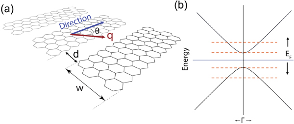
For the plasmonic characteristics of GeNSs (Fig. 1(a)), we follow the approach introduced by Popov et al.[15]. Specifically, we calculate the plasmon frequency () using the following expression:
Figure 1.(Color online) (a) Schematic representation of GeNSs. (b) Hypothetical low-energy band structure of GeNSs, showing the modulation of charge carrier density by shifting the Fermi level (orange dashed lines).
In Eq. (4), the effective electron mass is represented as m*, the background dielectric constant is represented as ε, the 2D carrier density is represented as N2D, the negative particle charge is represented as e, the plasmon excitation angle is represented as θ, the momentum along the strip direction is represented as q, and the particle relaxation rate is represented as v. N2D can also be expressed as: N2D = N1D/d. N1D is the 1D carrier density of a single strip and is the distance between strips (Fig. 1(a)).
Eq. (4) effectively describes the surface plasmon behavior, which is the most interesting and adjustable resonance mode for plasmonic applications. We can use this equation to calculate the propagation of surface plasmon frequencies in GeNSs, as long-established by experimental observations[27]. We solely refer to the surface plasmon studied throughout this work as the "plasmon" to keep the terminology simple.
As a result, by including the group velocity () of germanene in Eq. (4), it is feasible to determine the effective electron mass[28]:
and the value of the bandgap () of an individual strip can be determined as[28]:
where the Planck constant is commonly represented by .
It is important to note that a key component of Eq. (4) and the foundation of the semi-analytical model is the group velocity of germanene, which in the present case is calculated at the Fermi level () and around the K point, via GW or DFT calculations. This approach can be used to construct a linear fit of the and energy bands to yield behavior that is similar to the Dirac cone approximation[29, 30], denoted as follows:
in which, the plus/minus () sign represents the -lowest-conduction band and -highest-valence band, and is the vector momentum.
Now, it is crucial to take into account the quasi-1D confinement of carriers, which results in many energy sub-bands (). Then, to obtain the electron band structure of the systems under investigation, we use the following expression[29−31]:
Here, the sub-band integer index is denoted as (), and the parallel wavevector is denoted as .
Interestingly, Eq. (8) shows parabolic-electron band dispersions at the point (Fig. 1(b)), which are predominant in narrow-wide GeNSs and start to be less pronounced by increasing the strip width ().
To further individualize the examination of plasmonic characteristics in a given situation, Eq. (4) can be adapted using the well-known concepts of (i) the Fermi energy (Fermi level, Fig. 1(b)) or (ii) the intrinsic semiconductor behavior. In the first case, the resulting expression is:
and in the second case, it is expected that is located in the middle of the forbidden energy region, i.e., bandgap, resulting in:
in which, Ev and Ec denote the valence and conduction band edges, Nv and Nc denote the effective DOS in the valence and conduction bands, kB denotes the Boltzmann constant, and T denotes the absolute temperature.
Eq. (4) can therefore be stated in terms of both the required Fermi level shift and the desired temperature.
Because Eq. (4) is straightforward, the radicand turns negative when the damping is really large. This numerical impact can be explained in terms of many physical processes, such as scattering, absorption, and radiation, which cause plasmon energy to be lost. The plasmon response can then shift in the direction of larger momenta, which is equivalent to a higher frequency or shorter wavelength. We employ the idea of the complex dielectric function[32], to more clearly understand this phenomenon.
where stands for the imaginary part of the out-of-phase response and stands for the real part of the in-phase response[19]. Eq. (11) states that plasmons can be found by searching for zeros in the real part at frequencies where the imaginary part is either negligible or zero. If this need is not met, plasmons are not allowed.
Plasmon spectrum using the Lorentz function
The typical method of a spectral line profile can be applied to display the maximum of the plasmon peak, i.e., the plasmon spectrum for chosen values of , as follows:
Here, L denotes the Lorentzian function, ωo denotes the maximum transition energy/frequency derived from data generated by Eq. (4), ω denotes the energy/frequency sample of interest, and capital W denotes the full width at half maximum (FWHM).
For all spectra, the value of FWHM is set at 0.25 THz. The chosen FWHM value of 0.25 THz is considered reasonable and suitable for describing the underlying physical mechanisms that potentially contribute to the broadening of the plasmon spectra. Various factors, including temperature effects, impurities and scattering processes, can contribute to spectral broadening. However, these specific effects are currently under analysis and will be thoroughly addressed in future work. Using an FWHM value that encompasses a plausible range of broadening mechanisms, allows for preliminary characterization of the spectral features and aids in interpreting the data. The decision to select this value acknowledges the ongoing investigation into the specific contributions of these factors and recognizes that further research is needed to fully understand and quantify their effects.
A typical paradigm for describing spectroscopic characteristics in physical systems, including ions, molecules, atoms, and now GeNSs, is the Lorentzian line function. For, , and , this analysis employs frequency units, as is typical for collective excitation spectra[33]. It should be noted that the maximum of the plasmon peak may move when samples are supported on metallic substrates due to core–electron excitations[34], although this does not apply to suspended GeNSs. Additionally, it is not anticipated that the plasmon spectrum in GeNSs will be a straightforward Lorentzian peak, but this method successfully illustrates how plasmons are controlled in the systems under consideration.
Results and discussions
The case of suspended germanene
First, it is crucial to comprehend the importance of group velocity, which refers to the velocity at which electric charges like electrons or holes move through a material. Like graphene, germanene is expected to exhibit a high group velocity, making it well-suited for use in high-speed electronic devices, integrated circuits, and photovoltaic devices. Accurately measuring the group velocity of germanene can provide valuable insights into its electronic properties, aiding in optimizing device performance.
The estimated values for the group velocity of germanene from the GW ( m·s−1) and DFT ( m·s−1) computations are shown in Table 1. The GW value was underestimated by the DFT computation by 24.93%. Unfortunately, the experimental group velocity of germanene remains uncertain to date, with calculations of this value limited to conventional DFT predictions, which align with the estimated value presented in our study. In particular, determining the experimental group velocity in germanene is challenging due to several factors such as:
Table Infomation Is Not Enable
(i) Experimental challenges: Measuring the charge carrier velocity requires sophisticated experimental techniques that are often intricate and expensive. Germanene, a two-dimensional allotrope of germanium, is a relatively new material, and experimental methods tailored specifically for germanene might still be under development or refinement.
(ii) Sample quality: The quality and purity of the germanene sample significantly impact the measurement of charge carrier velocity. Even minor impurities or defects in the material can affect its electronic properties and introduce uncertainties in the velocity measurements.
(iii) Mobility and scattering: The charge carrier velocity depends on the mobility of charge carriers within the material. Various scattering mechanisms, such as lattice defects, impurities, and phonon scattering, can hinder the motion of charge carriers, leading to a reduction in their velocity. Identifying and characterizing these scattering mechanisms in germanene can be challenging.
(iv) Temperature and environmental effects: The charge carrier velocity in materials can be temperature-dependent. Factors such as ambient temperature, pressure, and the presence of other gases or materials in the environment can influence the charge carrier velocity, making its determination more complex.
With this in mind, we compare the values obtained at the same theoretical level for graphene (GW-gr), showing that the group velocity of germanene is 37.21% less than that of graphene. It is interesting to note that the GW-group velocity of graphene came very near to the experimental value (Exp-gr) and just slightly overstated it by 1.64%[30]. This implies that the GW approximation can be used to accurately estimate the group velocity of graphene as well as germanene, and it also suggests that comparable experimental outcomes from future studies are likely to be obtained.
The investigation of the full-electron band structure of freestanding germanene is then carried out using both DFT and GW calculations on a grid of . Fig. 2 provides a comparative analysis of the electron band structure between DFT computations (depicted in black) and quasi-particle GW (represented in red) computations, offering a comprehensive understanding of the exchange and correlation effects. Indeed, the exchange and correlation effects have led to non-trivial modifications in the band shapes and dispersions. Significantly, the gaps at the M (1.8 2.14 eV) and Γ (0.96 1.19 eV) points demonstrate an increase of up to 16% and 20% respectively. Furthermore, there is an increase in the energy of the linear dispersion around the K point, suggesting a raised group velocity of germanene, as indicated in Table 1. When comparing the two theoretical levels, it is worth noting that this effect is also seen in freestanding graphene (GW vs. DFT), as depicted in Fig. S1.
Figure 2.(Color online) Full-electron band structure of freestanding germanene along the path by using the approach of the GW approximation (continues red) and conventional DFT (dashed black) computations.
In Fig. 3(a), we examine the Dirac point region by analyzing energy-momentum data from the conduction () and valence () bands of freestanding germanene with the second grid of , and obtained through GW calculations.
Figure 3.(Color online) (a) Low-energy band structure of freestanding germanene in the vicinity of the Fermi level and K-point. The energy bands and resemble green and black, respectively. The linear fit is indicated by the cyan line. (b) Color plot depicting the group velocity of suspended germanene near the K point. The plot shows how the carrier velocity changes with energy and wavevector. The group velocity with negative values is the carrier velocity in the valence band.
Based on these data, we calculated the group velocity by a line fit (continues cyan, Fig. 3(a)), as follows:
It is observed that a perfect linear electron-energy dispersion (Fig. 3(a)) is closely aligned with the Dirac cone approximation (Eq. (7)) within a specific wave vector range (0.04 Å-1 ) and energy window (0.15 eV).
As indicated by the fading of the bright lines, Fig. 3(b) showcases the linear behavior of the group velocity within a smaller energy range (±0.12 eV, intense lines). This result is important because it set boundaries for the semi-analytical model (~30 THz), which is dependent on a Dirac-like linear relationship. DFT calculations yield similar results, which point to a limit of about 0.10 eV (~25 THz). Understanding the electronic characteristics of germanene and its possible plasmonic uses at THz frequencies requires knowledge of this crucial information.
The electronic characteristics of GeNSs
The link between bandgap and strip width is demonstrated to be inversely proportional in Eq. (6). As expected, the bandgap value drops exponentially with strip width. The bandgap value would eventually approach zero (), similar to germanene (Fig. 3(a)), and its associated structural and electronic features would progressively return if the strip width were infinite ().
The exponential drop in bandgap is then displayed in Fig. 4 as an illustration of this relationship, regardless of whether the group velocity value was calculated using DFT (blue trend) or GW (red trend). In narrow GeNSs with a width of 10 to 50 nm (Fig. 4(a)), the bandgap decreases from 0.3 to 0.05 eV, emphasizing the impact of the strip width on the bandgap. Conversely, in wide GeNSs with strip widths of 100 to 500 nm (Fig. 4(b)), the bandgap reduces from a range of 30 to 5 meV, exhibiting a six-fold reduction in the bandgap for both scenarios. The ensuing discussions will focus on the insights obtained through GW calculations, which have enabled the proper determination of the group velocity of germanene (see Section 3.1).
Figure 4.(Color online) Variation of bandgap in (a) narrow GeNSs (10−50 nm wide) and (b) wide GeNSs (100−500 nm wide). The estimated bandgaps via GW-group velocity are compared with those values via DFT-group velocity.
Table 2 presents the effective electron masses and bandgaps for different nanostrips with varying widths. A notable trend emerges from the data: As the nanostrip width increases, the bandgap becomes narrower. For instance, the 100 nm wide nanostrip exhibits a bandgap of approximately 29 meV, whereas the 500 nm wide nanostrip demonstrates a bandgap of around 6 meV, highlighting this decreasing trend in the bandgap with an increasing nanostrip width.
Table Infomation Is Not Enable
Furthermore, it is worth noting that the effective electron masses follow a similar pattern when comparing nanostrips of the same width, such as the 100 and 500 nm wide strips. The determined values of effective electron mass for the different nanostrips align with experimental results and hypotheses for systems associated with graphene[35], with the magnitudes falling within the same order. These findings strongly suggest that the characteristics of GeNSs are comparable to those of graphene nanostrips.
We now show the electron band structure (Figs. 5(a) and 5(c)) and DOS (Figs. 5(b) and 5(d)) of the 100 and 500 nm wide nanostrips, respectively, at an energy range of about 70 meV. Understanding their electronic properties and their possible uses in numerous industries is made easier by this analysis. For the semiconductor sector, for instance, GeNSs with a bandgap of around 1.1 eV, comparable to silicon, would be advantageous. Instead, GeNSs with widths ≥100 nm are particularly attractive for nanophotonic and nanoplasmonic applications. As noted, these types of nanostrips have a bandgap in the range of a few meV (Table 2).
Figure 5.(Color online) Electron band structure and DOS of GeNSs with widths of (a), (b) 100 nm and (c), (d) 500 nm. The smoothed curve of the histogram is shown by the red line.
Comparatively, it can be seen that for both 100 and 500 nm wide systems, there is a quadratic band dispersion of the conduction and valence bands close to the (zero) point. It should be emphasized that we have kept the effective electron mass constant for all bands; Eq. (8) has only changed the sub-band index (). Although the effective electron masses of each band can be precisely calculated using ab initio techniques, the fundamental problem is that the systems examined in this work are too complex for contemporary computers to handle. This is where the semi-analytical model excels and yields plausible results.
Hence, we can see that the 500 nm wide nanostrip (Fig. 4(c)) exhibits a significantly higher number of bands than the 100 nm wide nanostrip (Fig. 4(d)). It is also important to note that as nanostrip width increases, the energy gap between the bands narrows and they tend to converge, whenever feasible, to the same energy state. This is similar to what we see in germanene, which has the equivalent and bands (Figs. 2 and 3(a)), where the bands tend to converge to the same energy state.
Figs. 5(b) and 5(d), respectively, show the DOS of the nanostrips with widths of 100 and 500 nm, with multiple peaks corresponding to the bands in the electron band structure plot. It is worth noting that a narrower bandgap of the system can be observed and can result from smoothing the DOS histogram (red curve). For instance, the bandgap of a nanostrip with a width of 100 nm is roughly 23 meV, while one with a width of 500 nm is about 4 meV, resulting in bandgap reductions of 20% and 31%, respectively.
The effect of carrier density
It is important to recognize that the parameters indicated in Eq. (4) can be introduced irrespective of any particular physical context before diving further into an investigation of the plasmonic properties. By just using experimental data to calculate these parameter values or depending on forecasts from more sophisticated models, this work tries to avoid the superficial manipulation of these parameters. Understanding and regulating these variables is essential in plasmonics because they have a big impact on the plasmon frequency and plasmon dispersion. Indeed, experiments can be modified to create improved plasmonic devices by optimizing these parameters. On the other hand, Fei et al.[13] have successfully fabricated graphene nanostrips with widths similar to those examined in this study (i.e., 155, 270, 380, and 480 nm), providing a relevant reference for our analysis.
The effect of charge carrier density on the plasmonic characteristics of GeNSs is the main topic of this section in light of the foregoing. According to earlier research, isolated graphene nanostrips have a charge carrier density of about cm−1[36, 37], although this value may change based on doping, strip length, strip width, or another related parameter.
For GeNSs, comparable outcomes are anticipated. The charge density can then be adjusted to the desired value using the above formula (see Section 2.3): (see Table 3). In this situation, it is evident that as the distance between neighboring nanostrips grows, the charge density falls. For instance, the charge density falls by an order of magnitude if the vacuum distance between nanostrips is increased from 10 to 100 nm. However, it should be emphasized that in this instance, the Fermi level (), which ranges from 0.37 eV ( nm) to 0.12 eV ( nm), only falls by approximately three times.
Table Infomation Is Not Enable
Fig. 6(a) illustrates the dispersion of the plasmon frequency-momentum concerning the reciprocal wave vector () for a 100 nm wide nanostrip. The plasmon dispersion in GeNSs exhibits a characteristic similar to , as anticipated for 2D nanomaterials such as germanene or graphene. Notably, an intriguing observation is that the plasmon frequency and dispersion decrease as the distance between neighboring nanostrips increases from 10 to 100 nm. This effect can be attributed to the relationship between plasmon frequency and the square root of the charge density (~).
Figure 6.(Color online) The system under study corresponds to a 100 nm wide nanostrip (, = 0°, ). (a) Dispersion of the plasmon frequency-momentum as a function of the wave vector, considering different values of . (b) Plasmon spectra for selected values of momenta. (c) Density plot of the dispersion of the plasmon frequency as a function of carrier density versus wave vector.
Moreover, Table 3 shows that for a 100 nm wide nanostrip with a bandgap of a few meV (29 meV), a tight separation distance of 10 nm results in a high charge-carrier density ( cm−2) and a large Fermi level shift of 0.37 eV. As a consequence, we move our attention to the charge density of cm−2, which is a value that is frequently used in the modeling of 2D graphene-like materials. Surprisingly, at this charge carrier density, the Fermi level shift drops to just 0.12 eV, and a separation-vacuum distance of 100 nm is sufficient to consider GeNSs to be quasi-independent single 1D germanene systems.
Given this, Fig. 6(b) depicts the propagation of the plasmon peak for a 100 nm wide nanostrip with a carrier density of cm−2 at chosen momentum values between 0.1 and 3 THz, which corresponds to the frequency range where the majority of germanene-based plasmonic applications may take place.
Fig. 6(c), on the other hand, provides a thorough investigation of the impact of the charge density between to cm−2. The analysis yields three important findings:
(i) Forbidden areas for plasmons at momentum values close to 0 (purple region).
(ii) By increasing the charge density and momentum, the spectral weight also does.
(iii) At high carrier densities ( cm−2), plasmon responses can be observed up to roughly 30 THz (red region).
The effect of effective mass
The variable under investigation now is the effective electron mass, which depends on the bandgap and group velocity of freestanding germanene (Eq. (5)). Any variation in the effective mass can only be attributed to the bandgap since the group velocity employed in the computation ( m∙s−1) remains constant. The strip width determines the bandgap, according to Eq. (6). These results, which are shown in Table 2, will be further discussed in this section.
Fig. 7(a) shows a -like plasmon dispersion, and it is clear that as the nanostrip width is increased, the effective electron mass decreases, increasing in plasmon frequency. Given that the plasmon frequency is inversely related to the square root of the effective electron mass, ~, it is easy to comprehend this correlation. Table 2 illustrates how the effective electron mass decreases as the nanostrip widens.
Figure 7.(Color online) (a) Dispersion of the plasmon frequency-momentum as a function of the wave vector, considering different values of ) (see Table 2). The extra modeling parameters are = 0°, cm−2, and . (b) Plasmon spectra at cm−1 for different values of ). (c) Density plot of the dispersion of the plasmon frequency as a function of effective electron masses versus wave vector.
By showing that increasing the nanostrip width or lowering the effective electron mass results in an increase in plasmon frequency, Fig. 7(b) provides convincing proof of the control and tunability of the plasmon response. As is already noted, these spectra concentrate on a frequency range of 0.1 to 3 THz which is very important for germanene-based plasmonic applications. As a result, GeNS-based devices with a width size between 100 and 500 nm seem to be potential choices for these types of applications. Fig. 7(c) shows that there are no plasmon-forbidden zones and verifies that decreasing the effective electron mass raises the plasmon frequency by about 22 THz (the red region).
The effect of excitation angle
Fig. 8(a) investigates how the experimentally adjustable plasmon excitation angle affects a nanostrip that is 100 nm wide. It is crucial to bear in mind that the frequency of the plasmon drops as the plasmon excitation angle rises, suggesting that at an angle of 90°, there is no plasmonic response in the perpendicular direction. It is clear that by modifying this parameter, the plasmonic response for angles less than 90° can be tailored for particular uses in the frequency range of 0.1 to 3 THz (Fig. 8(b)). The plasmon response also moves towards lower frequency values as the angle is increased.
Figure 8.(Color online) (a) Dispersion of the plasmon frequency-momentum as a function of the wave vector, considering different values of . The current system corresponds to a 100 nm wide strip with fixed parameters as: cm−2, , and . (b) Plasmon spectra at cm−1 for selected values of . (c) Density plot of the dispersion of the plasmon frequency as a function of excitation angles versus wave vector.
Fig. 8(c) shows that there are regions where plasmons are not allowed and that these regions become more apparent as the angle increases. Interestingly, the extended purple zone shows that these forbidden regions may also be seen by increasing the momentum value. It is also crucial to emphasize that tiny angles produce the highest spectrum intensity, which results in a plasmonic response of almost 10 THz (the red region).
The effect of electron relaxation rate
Finally, we concentrate on a crucial factor, the electron relaxation rate in a 100 nm wide nanostrip. The values for electronic mobility and plasmon relaxation rate (γ, damping), which are displayed in Table 4, depend heavily on this parameter. Eq. (4) can be used to explicitly determine the plasmon frequency in terms of plasmon damping by utilizing the formula to compute the damping. As well, it is possible to determine the electron mobility () by applying the formula , where τ is the electron relaxation time, along with additional factors from Eqs. (9) and (10).
Table Infomation Is Not Enable
The effect of the electron relaxation rate on a 100 nm wide nanostrip is examined as an illustration in Fig. 9. It can be shown in Fig. 9(a) that the dispersion of the plasmon frequency continues to be inversely related to . Two more occurrences are seen, however, as electron relaxation rates rise:
Figure 9.(Color online) (a) Dispersion of the plasmon frequency-momentum as a function of the wave vector (, cm−1), considering different values of electron relaxation rate. (b) Maximum of the plasmon peak at cm−1 for selected values of electron relaxation rate. (c) Density plot of plasmon frequency-momentum dispersion as a function of electron relaxation rate and wave vector. The analyzed system corresponds to a 100 nm wide nanostrip ( cm−2, , = 0°).
(i) The plasmonic response shifts in favor of greater momentum values.
(ii) The plasmon response frequency sharply decreases.
In addition to the influence of the electron relaxation rate, Fig. 9(b) reveals that even a 100 nm wide nanostrip, when subjected to this effect, exhibits plasmon responses in the frequency range of 0.1 to 3 THz, highlighting the adjustability of its plasmonic features. Furthermore, Fig. 9(c) demonstrates the presence of forbidden plasmon areas that become more pronounced as the electron relaxation rate and momentum increase (the purple region). Consistent with previous observations, an increase in the electron relaxation rate leads to a significant decrease in the plasmon frequency. For instance, in a 100 nm wide nanostrip, the plasmon frequency reaches its maximum intensity at approximately 2 THz (the red region).
Taking all these results in mind, one can conclude that Eq. (4) provides a comprehensive understanding of the plasmon response, encompassing its frequency, dispersion, and various other influencing characteristics. By meticulously evaluating these variables, one can independently or collectively adjust them to customize the plasmon response and plasmons dispersion according to specific application requirements.
Comparison with available literature
While not our main objective, we tested the semi-analytical model using previous predictions and evidence of graphene and germanene nanoribbons less than 100 nm wide.
For comparison with experimental values of the bandgap[38] (Fig. S2(a)) with those obtained from Eq. (6) (the solid black line), we employed graphene nanoribbons with widths ranging from 15 to 90 nm. The results revealed a considerable level of agreement between the experimental and predicted values. In addition to the significant influence of the strong interaction between quantum confinement and edge states, we further compared our predictions to those derived using the GW approximation for various graphene nanoribbons[39]. Remarkably, an impressive level of agreement was observed for nanoribbons wider than 1.5 nm.
On the other hand, the bandgap of narrow-wide germanene nanoribbons has been estimated by Xu[40] and Acun[41] to range from 0.3 to 1.5 eV for ribbon widths less than 10 nm. Strikingly, the semi-analytical model (Fig. S3) produced similar results.
After obtaining these results, we have chosen to apply the semi-analytical model to determine the bandgap of a 2.7 nm wide graphene nanoribbon that has been experimentally observed by Kiraly et al.[42] on Ge(001). Our findings suggest that this system exhibits a bandgap of approximately 1.7 eV (Fig. S4(a)). The DOS is shown in Fig. S4(b). It is impressive that the smoothed curve of the DOS histogram can perfectly reproduce the results obtained by scanning tunneling spectroscopy (STS) (Fig. S4(c)).
According to Ref. [14], the freestanding narrow-wide five-armchair graphene nanoribbon (5AGNR) is reported to possess an effective electron mass of , as viewed from the perspective of plasmonics. By incorporating this value into Eq. (4) and considering a change in the Fermi level of up to 0.3 eV (corresponding to cm−2), we can explicitly establish this relationship and observe a perfect agreement between the semi-analytical model and TD-DFT in terms of the plasmon frequency-momentum dispersion. However, it is worth noting that deviations emerge when higher doping values (0.4 eV) are considered.
Conclusions
In conclusion, our study employed a semi-analytical model utilizing the group velocity of freestanding germanene as a key input. Through DFT calculations, we determined the charge carrier velocity to be m·s−1. Subsequently, the GW approximation was utilized to refine this result, yielding m·s−1. By incorporating this GW-group velocity value into the proposed modeling strategy, we investigated the electronic characteristics and THz plasmons in GeNSs with a width of ≥100 nm. Our comprehensive analysis encompassed a wide range of parameters and variables, aiming to provide a thorough understanding of the behavior and properties exhibited by these nanostrips.
Based on our research findings, nanostrips with a window width of 100−500 nm exhibit bandgap values in the few meV range from 29 down to 6 meV, respectively. Additionally, our investigation reveals that the effective electron mass in these systems varies from for 100 nm wide strips to for 500 nm wide strips. Regardless of the strip width, the electron band structure of these nanostrips is characterized by an almost parabolic-like band dispersion pattern, providing detailed insights into their electronic behavior.
An extensive investigation into the plasmonic properties of various nanostrips has been made feasible by utilizing a semi-analytical model in our study. By considering factors such as strip width, charge carrier density, plasmon excitation angle, and electron relaxation rate, we have achieved a comprehensive understanding of their impact. Our research demonstrates that precise control and tailored customization of plasmonic characteristics to meet specific application requirements can be attained by independently or collectively adjusting these parameters. This finding opens up new possibilities for achieving the desired plasmon resonance through strategic parameter manipulation, enabling us to meet the unique needs of various applications. An important observation from our study is that all the nanostrips we examined demonstrate a -like plasmon dispersion in the THz regime (30 THz), with the corresponding plasmon THz frequency being adjustable. Moreover, when the plasmon response is shifted to higher momentum levels, certain locations become unsuitable for sustaining plasmons. These findings emphasize the potential for manipulating and modulating plasmons in GeNSs (Germanium nanostrips), rendering them highly appealing for tailoring plasmonic characteristics according to specific requirements. This ability to control plasmons in GeNSs opens up promising avenues for customizing and optimizing plasmonic behavior to meet diverse application needs.
Our research offers a thorough understanding of the electronic and plasmonic characteristics of GeNSs, which is essential for the creation of upcoming nanodevices. Future research targeted at verifying our findings can greatly benefit from the understanding gained from the present study.