• Acta Physica Sinica
  • Vol. 69, Issue 7, 078501-1 (2020)
Shi-Jian Dong1, Hong-Xia Guo1、2、3、*, Wu-Ying Ma3, Ling Lv4, Xiao-Yu Pan3, Zhi-Feng Lei2, Shao-Zhong Yue1, Rui-Jing Hao1, An-An Ju1, Xiang-Li Zhong1, and Xiao-Ping Ouyang1、3
Author Affiliations
  • 1School of Materials Science and Engineering, Xiangtan University, Xiangtan 411105, China
  • 2State Key Laboratory of Science and Technology on Reliability Physics and Application of Electronic Component, CEPREI, Guangzhou 510610, China
  • 3Northwest Institute of Nuclear Technology, Xi’an 710024, China
  • 4Key Laboratory of Wide Bandgap Semiconductor Materials and Devices, Ministry of Education, School of Microelectronics, Xidian University, Xi’an 710071, China
  • show less
    DOI: 10.7498/aps.69.20191557 Cite this Article
    Shi-Jian Dong, Hong-Xia Guo, Wu-Ying Ma, Ling Lv, Xiao-Yu Pan, Zhi-Feng Lei, Shao-Zhong Yue, Rui-Jing Hao, An-An Ju, Xiang-Li Zhong, Xiao-Ping Ouyang. Ionizing radiation damage mechanism and biases correlation of AlGaN/GaN high electron mobility transistor devices[J]. Acta Physica Sinica, 2020, 69(7): 078501-1 Copy Citation Text show less
    AlGaN/GaN HEMT devices’ cross-section.
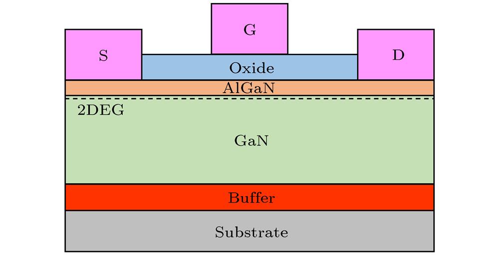
    Fig. 1. AlGaN/GaN HEMT devices’ cross-section.
    AlGaN/GaN HEMT devices’ low frequency noise measurement system.
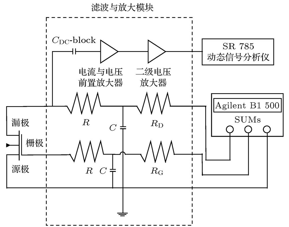
    Fig. 2. AlGaN/GaN HEMT devices’ low frequency noise measurement system.
    The output characteristic curve (a) and transfer characteristic curve (b) of the AlGaN/GaN HEMT device before and after irradiation under the zero-bias.
    Fig. 3. The output characteristic curve (a) and transfer characteristic curve (b) of the AlGaN/GaN HEMT device before and after irradiation under the zero-bias.
    Charge distribution patterns of AlGaN/GaN HEMT devices: (a) The off and semi-on states; (b) zero-bias.
    Fig. 4. Charge distribution patterns of AlGaN/GaN HEMT devices: (a) The off and semi-on states; (b) zero-bias.
    Normalized channel current noise power spectral density in the AlGaN/GaN HEMT devices before and after irradiation: (a) OFF state; (b) SEMI-ON state; (c) zero-bias.
    Fig. 5. Normalized channel current noise power spectral density in the AlGaN/GaN HEMT devices before and after irradiation: (a) OFF state; (b) SEMI-ON state; (c) zero-bias.
    Normalized channel current noise power spectral density versus overdrive voltage in the AlGaN/GaN HEMT devices before and after irradiation: (a) OFF state; (b) SEMI-ON state; (c) zero-bias (dot: measured value; continuous line: fitted value).
    Fig. 6. Normalized channel current noise power spectral density versus overdrive voltage in the AlGaN/GaN HEMT devices before and after irradiation: (a) OFF state; (b) SEMI-ON state; (c) zero-bias (dot: measured value; continuous line: fitted value).
    Normalized channel current noise power spectral density versus channel current in the AlGaN/GaN HEMT devices before and after irradiation: (a) OFF state; (b) SEMI-ON state; (c) zero-bias (f = 25 Hz, dot: measured value; continuous line: fitted value).
    Fig. 7. Normalized channel current noise power spectral density versus channel current in the AlGaN/GaN HEMT devices before and after irradiation: (a) OFF state; (b) SEMI-ON state; (c) zero-bias (f = 25 Hz, dot: measured value; continuous line: fitted value).
    Extracted spatial distribution of trapped charges in the AlGaN/GaN HEMT devices’ barrier layer: (a) OFF state; (b) SEMI-ON state; (c) zero-bias.
    Fig. 8. Extracted spatial distribution of trapped charges in the AlGaN/GaN HEMT devices’ barrier layer: (a) OFF state; (b) SEMI-ON state; (c) zero-bias.
    VGS/V VDS/V
    关态(OFF)–3.00.5
    半开态(SEMI-ON)–1.90.5
    零偏(zero-bias)00
    Table 1. The biases set of AlGaN/GaN HEMT device irradiation experiment.
    关态(OFF)半开(SEMI-ON)零偏(zero-bias)
    ΔIDSsat/% –26.00–31.42–36.28
    Δgmmax/% –22.86–34.58–52.94
    Table 2.

    Variation of saturation drain current and maximum transconductance before and after irradiation in AlGaN/GaNHEMT devices with different biases.

    不同偏置下AlGaN/GaN HEMT器件辐照前后饱和漏电流与最高跨导的变化

    关态 (OFF) 半开态 (SEMI-ON) 零偏 (zero-bias)
    0 rad(Si)3.20 × 10–142.65 × 10–143.18 × 10⁻¹⁴
    1 Mrad(Si)4.21 × 10–143.85 × 10–145.16 × 10⁻¹⁴
    Table 3.

    Flat-band voltage noise power spectral density in the AlGaN/GaN HEMT devices before and after irradiation under different biases (in V2·Hz–1).

    不同偏置下AlGaN/GaN HEMT器件辐照前后平带电压噪声功率谱密度(单位: V2·Hz–1)

    关态 (OFF) 半开态 (SEMI-ON) 零偏 (zero-bias)
    0 rad(Si)4.106 × 10173.400 × 10174.080 × 1017
    1 Mrad(Si)5.402 × 10174.940 × 10176.621 × 1017
    ΔNt/% 31.5645.2962.28
    Table 4.

    The defect density in the AlGaN/GaN HEMT devices before and after irradiation under different biases (in cm–3·eV–1).

    不同偏置下AlGaN/GaN HEMT器件辐照前后缺陷密度(单位: cm–3·eV–1)

    Shi-Jian Dong, Hong-Xia Guo, Wu-Ying Ma, Ling Lv, Xiao-Yu Pan, Zhi-Feng Lei, Shao-Zhong Yue, Rui-Jing Hao, An-An Ju, Xiang-Li Zhong, Xiao-Ping Ouyang. Ionizing radiation damage mechanism and biases correlation of AlGaN/GaN high electron mobility transistor devices[J]. Acta Physica Sinica, 2020, 69(7): 078501-1
    Download Citation