• Acta Physica Sinica
  • Vol. 69, Issue 7, 078501-1 (2020)
Shi-Jian Dong1, Hong-Xia Guo1、2、3、*, Wu-Ying Ma3, Ling Lv4, Xiao-Yu Pan3, Zhi-Feng Lei2, Shao-Zhong Yue1, Rui-Jing Hao1, An-An Ju1, Xiang-Li Zhong1, and Xiao-Ping Ouyang1、3
Author Affiliations
  • 1School of Materials Science and Engineering, Xiangtan University, Xiangtan 411105, China
  • 2State Key Laboratory of Science and Technology on Reliability Physics and Application of Electronic Component, CEPREI, Guangzhou 510610, China
  • 3Northwest Institute of Nuclear Technology, Xi’an 710024, China
  • 4Key Laboratory of Wide Bandgap Semiconductor Materials and Devices, Ministry of Education, School of Microelectronics, Xidian University, Xi’an 710071, China
  • show less
    DOI: 10.7498/aps.69.20191557 Cite this Article
    Shi-Jian Dong, Hong-Xia Guo, Wu-Ying Ma, Ling Lv, Xiao-Yu Pan, Zhi-Feng Lei, Shao-Zhong Yue, Rui-Jing Hao, An-An Ju, Xiang-Li Zhong, Xiao-Ping Ouyang. Ionizing radiation damage mechanism and biases correlation of AlGaN/GaN high electron mobility transistor devices[J]. Acta Physica Sinica, 2020, 69(7): 078501-1 Copy Citation Text show less

    Abstract

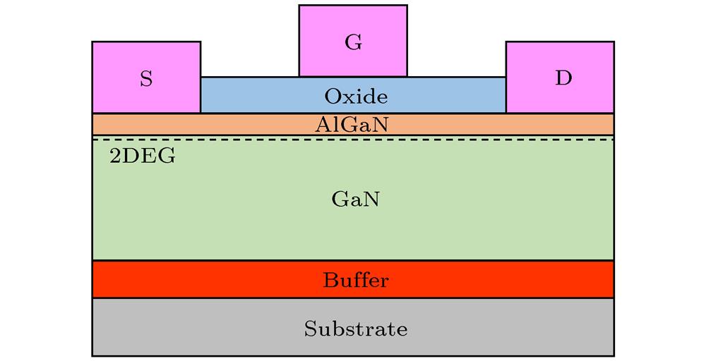
    In this paper, the total dose effect on AlGaN/GaN high-electron-mobility transistor (HEMT) devices after 60Co γ-ray irradiation with a total dose of 1 Mrad(Si) was investigated at different biases (VGS = –3 V, VDS = 0.5 V; VGS = –1.9 V, VDS = 0.5 V; VGS = 0 V, VDS = 0 V). The experimental results were analyzed using 1/f low-frequency noise and direct current electrical characteristics. The electrical parameters degraded mostly under zero bias condition because of the radiation-induced defect charge of the oxide layer and the interface state. Wherein, the saturation drain current was reduced by 36.28%, and the maximum transconductance was reduced by 52.94%. The reason was that the oxide dielectric layer of AlGaN/GaN HEMT devices generated electron-hole pairs under γ-ray irradiation, and most of the electrons were quickly swept out of the oxide region corresponding to the gate-source and gate-drain spacer regions, and most of the holes remained in the oxide. Under the action of the built-in electric field, holes slowly moved towards the interface between the oxide and AlGaN, which depleted the two-dimensional electron gas of the channel.According to the McWhorter model, the low-frequency noise in the AlGaN/GaN HEMT devices results from random fluctuations of carriers, which are caused by the capture and release processes of carriers by traps and defect states in the barrier layer. The extracted defect densities in AlGaN/GaN HEMT devices increased from 4.080 × 1017cm–3·eV–1 to 6.621 × 1017cm–3·eV–1 under the condition of zero bias, and the result was in good agreement with test results of the direct currentelectrical characteristics. The damage mechanism was the radiation-induced defect charge in the oxide layer and the interface state, which increased the flat-band voltage noise power spectral density of the AlGaN/GaN HEMT devices. According to the charge tunneling mechanism, the spatial distribution of defect in the barrier layer was extracted, and the result also proved that the densities of radiation-induced defect charges under zero bias were more than the other biases. The experimental results showed that zero bias was the worst bias for AlGaN/GaN HEMT devices irradiation.
    Shi-Jian Dong, Hong-Xia Guo, Wu-Ying Ma, Ling Lv, Xiao-Yu Pan, Zhi-Feng Lei, Shao-Zhong Yue, Rui-Jing Hao, An-An Ju, Xiang-Li Zhong, Xiao-Ping Ouyang. Ionizing radiation damage mechanism and biases correlation of AlGaN/GaN high electron mobility transistor devices[J]. Acta Physica Sinica, 2020, 69(7): 078501-1
    Download Citation