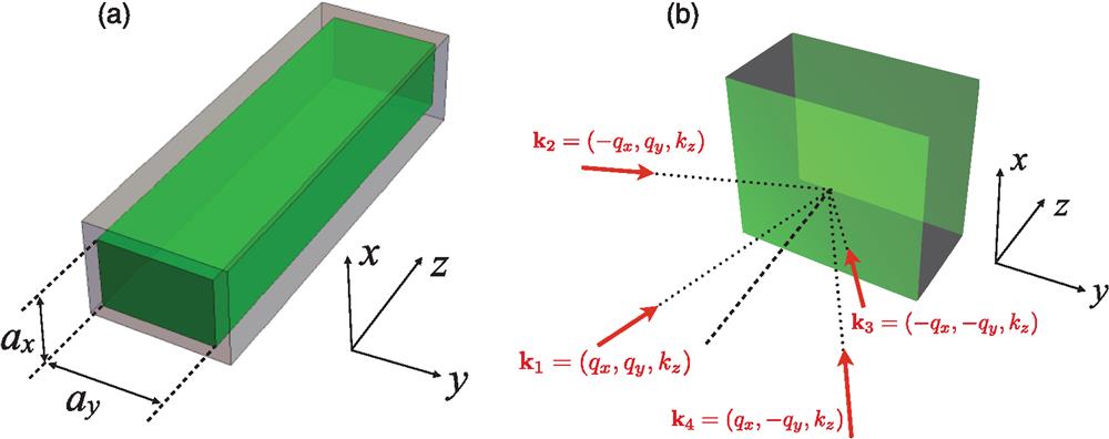
Fig. 1. (a) The schematics of the metal-clad waveguide with the core formed by a biaxial anisotropic dielectric material and (b) the corresponding standing wave pattern formed by the interference of several beams incident onto a slab of the biaxial anisotropic dielectric. Green color in (a) and (b) represents the anisotropic dielectric, whereas the gray region in (a) corresponds to the metallic cladding of the waveguide. For the wavevectors indicated in (b), , , with integer values of and the resulting field pattern is identical to that inside the perfect metal-clad waveguide in panel (a).
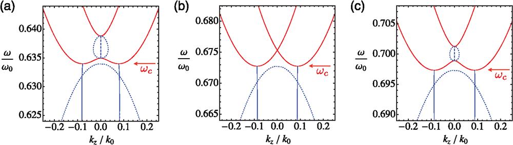
Fig. 2. The dispersion diagrams for the waves supported by sodium nitrite
, a biaxial anisotropic dielectric with the primary components of the dielectric permittivity tensor
20,28,
, and
. The frequency is shown in units of
and the wavenumber
in units of
, for (a)
,
; (b)
,
; and (c)
,
, where
is the free space wavenumber at the frequency
. The corresponding values of the critical frequency
are marked in each panel. For the waveguide system in
Fig. 1(a),
and
, where
and
are the positive integer numbers, whereas for the anisotropic dielectric slab geometry in
Fig. 1(b),
and
correspond to the magnitudes of the (in-plane)
and
components of the incident field wavevector. Note the Dirac point in (b) at the frequency
. Red lines represent the propagating modes, whereas blue curves correspond to the ghost waves, with dashed and dotted lines showing the real and the imaginary parts of the wavenumber
.
Fig. 3. The component of the electric field in the biaxial anisotropic dielectric, in either the waveguide or the slab geometry [see the schematics in Figs. 4(a) and 4(b)], as a function of the length . The dielectric occupies the range , , and . The surrounding medium is air, and the anisotropic dielectric is sodium nitrite . The inset shows the field in the logarithmic scale. Note the combination of the exponential decay and the oscillatory behavior, characteristic of the ghost waves.
Fig. 4. Evanescent field enhancement at the ghost resonance in the (a) waveguide and (b) slab geometry. Green region represents the biaxial anisotropic dielectric, blue is the surrounding dielectric medium, and orange is the high-index prism coupler. (c) The component of the electric field, with the linear scale in the main plot and the logarithmic scale in the inset. The green-shaded areas in (c) and its inset indicate the range occupied by the anisotropic dielectric medium. In this example, the anisotropic dielectric is sodium nitrite with the width , and the surrounding medium is dielectric with the permittivity of while and . Note the dramatic enhancement of the incident evanescent field in the anisotropic material.
Fig. 5. The frequency spectrum of the “transmitted” field , normalized to the amplitude of the incident field at [see the schematics in Figs. 4(a) and 4(b)], for the sodium nitrite biaxial crystal [green region in Fig. 4(a)], surrounded by an isotropic dielectric with the permittivity [shown in blue in Figs. 4(a) and 4(b)], with and . The length of the biaxial dielectric (red curve), (green curve), and (blue curve). The frequency is normalized to the value corresponding to the surface state at a single-sodium nitrite–isotropic dielectric interface, given by Eq. (15).
Fig. 6. (a) The schematic of the coordinate system used in the slab geometry of Fig. 4(b). Orange volume corresponds to the high-index prism coupler, and green layer is the biaxial dielectric. Light blue regions represent the isotropic dielectric surrounding the biaxial medium. Blue arrow shows the direction of the incident Gaussian beam, with the angle above the critical angle of the total internal reflection of the coupler—isotropic dielectric interface. (b) The modulus of the normal to the interface electric field component (in false-color representation) at the resonance condition. The incident beam direction is defined by the angles and , the biaxial medium is sodium nitrite , the high-index prism is made of gadolinium gallium garnet (), and the permittivity of the isotropic dielectric . The wavelength is , and the biaxial layer thickness .
Fig. 7. The evolution of the electromagnetic field in the slab geometry of Fig. 4(b), near the “ghost resonance,” with the incidence angle : (a) 46.42 deg, (b) 46.44 deg, (c) 46.46 deg, (d) 46.48 deg, and (e) 46.5 deg. The angle , the system spatial dimensions, and the material parameters are the same as in Fig. 6. Note that the entire sequence (a) to (e) corresponds to the variation of the incidence angle by .
Fig. 8. The surface state profile at the interface of isotropic dielectric () with biaxial anisotropic medium (). The red and blue lines, respectively, correspond to the and components of the electric field. The biaxial dielectric is sodium nitrite (, , and ), and the permittivity of the isotropic medium , whereas and . Note the simple exponential decay in the isotropic material and oscillatory behavior in the biaxial medium.
Fig. 9. The modulus of the electric field component (in false-color representation), for the resonant excitation of the (a) symmetric and (b) antisymmetric superpositions of the Dyakonov surface waves at the two biaxial–isotropic dielectric interfaces in the slab geometry of Figs. 4(b) and 6(a). The incidence angle is equal to (a) 46.4681 deg and (b) 46.4524 deg. The angle , the system spatial dimensions, and the material parameters are the same as in Figs. 6 and 7.