
Tian-Li He, Hong-Yuan Wei, Cheng-Ming Li, Geng-Wei Li. Comparative study of n-GaN transition group refractory metal Ohmic electrode [J]. Acta Physica Sinica, 2019, 68(20): 206101-1
- Acta Physica Sinica
- Vol. 68, Issue 20, 206101-1 (2019)
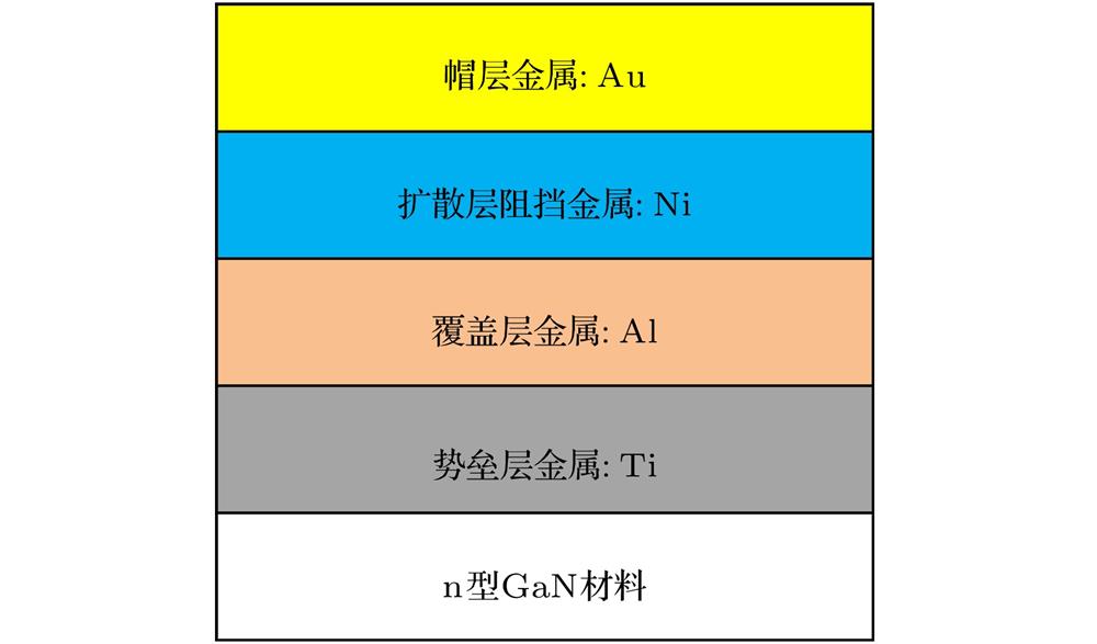
Fig. 1. Ti-based multilayer metal system most commonly used in n-type GaN ohmic contact目前最常应用于n型GaN欧姆接触的Ti基多层金属体系
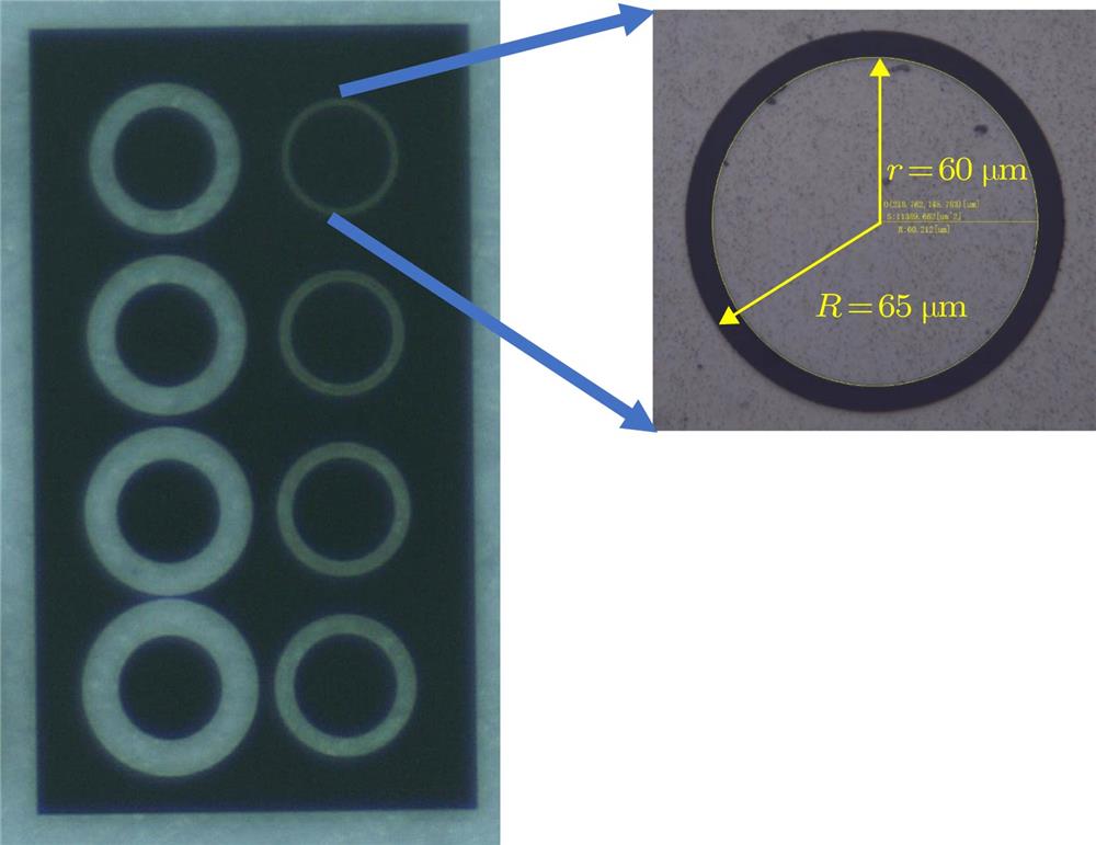
Fig. 2. The scheme of dot circular transmission line model (dot CTLM) in this experiment实验中用到的圆点型传输线模型(dot CTLM)结构
Fig. 3. I -V curve between Ti/Al, Hf/Al pads with 10 μm spacing anneales at different condition.
不同退火条件下Ti/Al, Hf/Al样品间距为10 μm的电极之间的I -V 曲线
Fig. 4. AES depth profiles of Hf/Al electrodes: (a) No annealing and (b) after annealing at 650 ℃ for 60 s in N2 ambient.
Hf/Al电极样品深度剖析的AES图 (a)未退火; (b) 650 ℃退火60 s
Fig. 5. Cross-sectional SEM image of each electrode: (a) Hf/Al, 650 ℃; (b) Hf/Al, 850 ℃; (c) Ti/Al, 650 ℃; (d) Ti/Al, 850 ℃各电极的截面SEM图像 (a) Hf/Al, 650 ℃; (b) Hf/Al, 850 ℃; (c) Ti/Al, 650 ℃; (d) Ti/Al, 850 ℃
Fig. 6. SEM image of each electrode annealed at 850 ℃ condition: (a) Hf/Al; (b) Ti/Al各电极在850 ℃条件下退火的表面SEM图 (a) Hf/Al; (b) Ti/Al
|
Table 1. Work function, melting point and resi-stivity of different metals.
|
Table 2. Specific contact resistivity of each electrode sample at different annealing conditions.

Set citation alerts for the article
Please enter your email address
© Copyright 2018-2021 | Chinese Laser Press. All Rights Reserved 沪ICP备15018463号-20