Abstract
Moiré superlattices are formed when overlaying two materials with a slight mismatch in twist angle or lattice constant. They provide a novel platform for the study of strong electronic correlations and non-trivial band topology, where emergent phenomena such as correlated insulating states, unconventional superconductivity, and quantum anomalous Hall effect are discovered. In this review, we focus on the semiconducting transition metal dichalcogenides (TMDs) based moiré systems that host intriguing flat-band physics. We first review the exfoliation methods of two-dimensional materials and the fabrication technique of their moiré structures. Secondly, we overview the progress of the optically excited moiré excitons, which render the main discovery in the early experiments on TMD moiré systems. We then introduce the formation mechanism of flat bands and their potential in the quantum simulation of the Hubbard model with tunable doping, degeneracies, and correlation strength. Finally, we briefly discuss the challenges and future perspectives of this field.Moiré superlattices are formed when overlaying two materials with a slight mismatch in twist angle or lattice constant. They provide a novel platform for the study of strong electronic correlations and non-trivial band topology, where emergent phenomena such as correlated insulating states, unconventional superconductivity, and quantum anomalous Hall effect are discovered. In this review, we focus on the semiconducting transition metal dichalcogenides (TMDs) based moiré systems that host intriguing flat-band physics. We first review the exfoliation methods of two-dimensional materials and the fabrication technique of their moiré structures. Secondly, we overview the progress of the optically excited moiré excitons, which render the main discovery in the early experiments on TMD moiré systems. We then introduce the formation mechanism of flat bands and their potential in the quantum simulation of the Hubbard model with tunable doping, degeneracies, and correlation strength. Finally, we briefly discuss the challenges and future perspectives of this field.Introduction
A flat band is formed when the electronic bandwidth is small and hence comparable or much smaller than the Coulomb interactions between electrons. The first well-known flat-band platform is the two-dimensional electron gases (2DEG) under a vertical magnetic field, where the electronic structure is quantized into discrete Landau levels (LLs)[1]. At low enough temperatures, the LL hosts the perfect flat band with its bandwidth solely determined by disorder broadening. The quenched kinetic energy promotes the effect of electron–electron interactions, giving rise to many exotic states and competing orders in a partially filled LL, such as the fractional quantum Hall effect[2] and non-Abelian states[3].
In recent years, the rise of twisted bilayer graphene (TBG) opens an entirely new avenue for exploring flat-band physics in moiré superlattices, without the need of applying external magnetic fields[7-11]. The flat band condition is fulfilled at certain twist angles (the so-called magic angles) due to the spatially varying interlayer hybridization (following the moiré periodicity) acting on the Dirac band structure[12]. Many intriguing phenomena including the unconventional superconductivity[8,13-14], correlated insulating states[7,15], and quantum anomalous Hall effect[16,17]have been discovered near the first magic angle (~1.05°), hence owing to the enhanced electronic correlations and notable nontrivial band topology. In the past few years, tremendous attention is paid to the moiré system constructed from different materials, such as 2D semiconductors[11,18-23], insulators[24], and magnetic materials[25-27].
Compared to TBG, the semiconducting TMDs-based moiré superlattices have several advantages. First, the flat bands can be realized in more relaxed conditions, e.g., in a much larger range of twist angles (typically smaller than ~4°–5°) for the twisted homobilayers[28-30]. This is partially due to the initially large effective masses (~0.5me, whereme is the free electron mass) near the band edge of the TMD monolayers. In contrast, the TBG has to be accurately near the magic angle (typically within 0.1° error) to support strong correlation effects, bringing inconvenience for sample preparation. Second, the TMD monolayers feature strong spin-orbit coupling and a variety of material choices, which can provide easy controllability on the degeneracy, lattice symmetry, and moiré potential landscapes[31,32]. The interplay between many degrees of freedom can potentially offer much richer interaction effects and more exciting physics. Third, some of the TMD materials are direct-bandgap semiconductors and have strong light-matter interactions. Hence many of the well-established optical methods (e.g., photoluminescence, reflection, and ultrafast spectroscopy) can be readily utilized to probe the electronic correlations and study the many-body effects in the TMD-based moiré superlattices. Fourth, a tight-binding approximation on the superlattice is demonstrated to be valid in describing the semiconducting TMD moiré materials, rendering them more applicable for studying the paradigmatic Hubbard model physics[5]. So even started later than the study of TBG, the TMD moiré systems have been able to attract a lot of attention both experimentally and theoretically in the last few years[11,18-23].
In this review, we focus on the fabrication and physical properties, especially the flat-band-related physics, of the TMD moiré systems (Fig. 1). We review the exfoliation of the monolayer flakes and the preparation of the moiré superlattice structures, followed by a brief introduction of moiré excitons observed in the TMD moiré systems. We overview the formation mechanism of flat bands and the consequential novel phenomena under various conditions, such as correlated insulating states at fractional fillings in the strong correlation limit, the Pomeranchuk effect at the intermediate electronic correlation strength, and the quantum anomalous Hall effect when the non-trivial topology is further included. The challenges and future perspectives of this field are discussed at the end of this review.
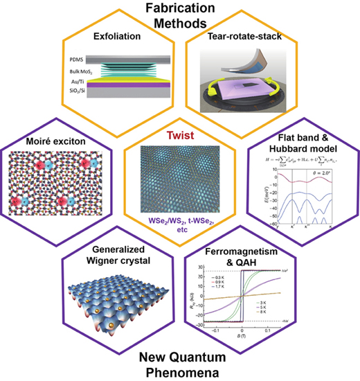
![(Color online) Schematic illustration of the topics of this review, including the fabrication methods and several distinctive properties of the twisted moiré materials[4–6]. ([4] Copyright 2018, American Physical Society. [5] Copyright 2018, American Physical Society. [6] Copyright 2021, Nature Publishing Group (NPG).)](/Images/icon/loading.gif)
Figure 1.(Color online) Schematic illustration of the topics of this review, including the fabrication methods and several distinctive properties of the twisted moiré materials[4–6]. ([4] Copyright 2018, American Physical Society. [5] Copyright 2018, American Physical Society. [6] Copyright 2021, Nature Publishing Group (NPG).)
Exfoliation of TMD and other 2D materials
There are two main different strategies for obtaining 2D materials. One is called the “bottom-up” strategy, which is represented by chemical vapor deposition (CVD) and molecular beam epitaxy (MBE). These sorts of methods can produce uniform materials at wafer scale and are therefore considered superior in obtaining large-area 2D crystals, but they often host strong coupling to the substrates[33-36]. Therefore, further complicated isolation and transfer skill are needed which may affect the intrinsic properties of 2D materials. In recent years, mechanical stacking of CVD-grown 2D materials has become an important technology for fabricating twisted van der Waals heterostructures at large scales[37]. However, the MBE-grown 2D materials usually have strong coupling with substrates, which makes it difficult to prepare heterostructures with clean interface.
The other strategy is called “top-down”, which is represented by mechanical exfoliation. After the first isolation of graphene, mechanical exfoliation has been widely used for preparing 2D crystals and their van der Waals heterostructures[38-41]. The high quality of these exfoliated 2D materials is the prerequisite for studying their intrinsic properties. As the most widely used method for preparing 2D crystals, exfoliation technology has made rapid progress over the past few years. Therefore, we will first review the mechanism and progresses of this “top-down” strategy before discussing the new phenomena in twisted TMD heterostructures.
The relevant interfacial interactions between 2D crystals and substrates are the primary parameter which need to be considered. The van der Waals force, affected by the contact distance and the dipole moment of the atoms, is the common interlayer interaction for most layered crystals and the interfacial interaction with a substrate. Once the interaction between the substrate and the outermost contacted layer exceeds the interlayer interaction in the crystal, monolayer flakes can be exfoliated from the bulk crystals. Therefore, reduction of the separation from the substrate and improvement of the dipolar interaction are the keys to enhance the exfoliation yield and flake size.
The cleanliness of the surface is an important factor that limits the exfoliation efficiency. Since most exfoliation is carried out in air, the extra molecules would be absorbed on the substrate and crystal surfaces. In this case, the contact distance between the layered crystal and the substrate will increase, resulting in the reduction of the interfacial van der Waals interaction. This issue is reported to be addressed through an oxygen plasma enhanced exfoliation method, which has been successfully used for yielding large-area (millimeter size) flakes of graphene and of the high-temperature superconductor Bi-2212[42,43]. The exfoliated large-area flakes bring great convenience to the preparation of heterojunctions by the tear-rotate-stack method.
The atomic structures of TMD materials (MoS2, WSe2, etc.) are different from graphene, with several atomic layers in the unit cell. For TMD crystals, the interfacial interaction between 2D crystal and substrate is mostly governed by the outermost atoms. Although oxygen plasma-enhanced exfoliation shows obvious improvement for graphene and Bi-2212, this method does not readily yield large-area MoS2 since the dipolar interaction between sulfur atoms in MoS2 and oxygen atoms in SiO2 is weak. Several groups have tried different ways to optimize the mechanical exfoliation of TMDs[44-46]. A universal exfoliation method using ultrathin gold adhesion layers was discovered in recent years, which shows great potential for preparing macroscopic scale 2D materials (millimeter to centimeter size,Fig. 2). More than 40 kinds of layered materials were exfoliated to monolayers, including TMDs, black phosphorus, FeSe, GaS, etc.[47]. For these layered crystals which contain the main group (group V, VI, VII) non-metals at the outermost layer, the interaction with the Au atom is larger than the interlayer van der Waals interaction, as confirmed by calculations and experimental results. This gold-enhanced exfoliation method can be used in the preparation of suspended 2D materials[48], and twisted van der Waals heterostructures by transfer and stacking[49].
Figure 2.(Color online) Mechanism of Au-film-assisted exfoliation technology and some examples of exfoliated 2D crystals. (a) Part of the periodic table, showing the elements involved in most 2D materials between groups 4 (IVB) and 17 (VIIA). Most of the layered crystals are composed of the elements with pink and green colors, which have strong interaction with Au. (b) Schematic of the interaction mechanism between layered crystal and Au. Once the interface interaction energy is larger than the interlayer interaction, monolayer flakes can be exfoliated. (c) Schematic illustration of the Au-film-assisted exfoliation process. (d) Optical images of large exfoliated 2D flakes[50]. Copyright 2022, Nature Publishing Group (NPG).
Though the Au-enhanced exfoliation technique provides an effective strategy for the preparation of large-scale 2D crystals, the high cost of gold hinders the widespread adoption of this technology. In addition, direct Au-TMD contact can significantly quench the photoluminescence (PL) emission in 2D semiconductors. It is therefore crucial to find alternative metals that can replace gold to achieve efficient exfoliation of 2D materials. Recently, a new one-step Ag-assisted method was reported[51], where the yield is comparable to the Au-enhanced exfoliation method (Fig. 3). In addition to the yield, the surface roughness of the Ag films on SiO2/Si substrate facilitates the generation of surface plasmons. Meanwhile, the strong coupling between 2D semiconductor crystals (e.g. MoS2, MoSe2) and Ag film leads to a unique PL enhancement which could be mainly attributed to the strong light-matter interaction as a result of extended propagation of surface plasmonic polariton (SPP). This Ag-assisted exfoliation method provides a lower-cost way to prepare large-area monolayer TMDs, which is also helpful for modulating SPP-matter interactions.
Figure 3.(Color online) Ag-assisted exfoliation procedures and optical images of exfoliated samples. (a) Schematic illustration of the exfoliation procedures. (b) Exfoliated macroscopic MoS2 and WS2 on 15 nm Ag film supported by SiO2/Si substrates, and bulk crystals on PDMS tapes. (c) Exfoliated macroscopic MoS2 supported by sapphire substrates. (d) Exfoliated MoS2 supported by elastic PET substrates. (e) Exfoliated MoS2 on Ag/epoxy/glass slide substrate. (f) Optical microscope images of some 2D crystals exfoliated on 15 nm Ag film, including MoS2, WS2, 1T-WTe2, and BP. (g) Optical microscope images of exfoliated millimeter size 2D crystals on 5 nm Ag film, including ReSe2, Fe3GeTe2, FeSe, and TaS2. (h, i) Optical microscope images of exfoliated millimeter size MoS2 on sapphire substrate and TS Ag, respectively. (j) Optical microscope and PL mapping images of exfoliated monolayer WS2 on 15 nm Ag film with hole array, the scale bars in the two images are 40 and 20μm, respectively[51]. Copyright 2022, Wiley Online Library.
2D materials are highly sensitive to substrates, interfaces and the surrounding environments. Suspended 2D materials are free from substrate-induced effects, thus providing an ideal approach to study their intrinsic properties. However, it is very challenging to prepare large-area suspended 2D materials with high efficiency. Recently, large-area suspended mono- and few-layer 2D materials were prepared on pretreatments of densely patterned hole array substrates with either oxygen-plasma or gold film deposition (Fig. 4)[48]. Multiple structural, optical, and electrical characterization methods were used to fully evaluate the improved performance of various suspended 2D layers. For example, new low frequency Raman modes were observed on suspended MoS2, with enhanced PL and second harmonic generation (SHG) signals were also discovered on suspended WS2 and WSe2[52]. This work provides an innovative and efficient route for fabricating suspended 2D materials, which will be broadly used for studying intrinsic properties of 2D materials and in applications of hybrid active nanophotonic and electronic devices.
Figure 4.(Color online) Fabrication process and characterization of suspended 2D materials. (a) Schematic images for preparing suspended samples. (b–d) Optical images of exfoliated graphene, MoS2 and WSe2 on different patterned substrates, including rectangle, Hall bar and circular hole structures. (e) PL mapping image of suspended monolayer WSe2[48]. Copyright 2022, Wiley Online Library.
Several different ways can be used to assemble moiré superlattices after preparing 2D materials by exfoliation or CVD methods. Tear-rotate-stack is the commonly used assembling technique to prepare twisted homobilayers with a designed twist angle[53].Fig. 5(b) present the fabrication process. First, a hemispherical handle substrate is fabricated from a small epoxy or polydimethylsiloxane (PDMS) droplet deposited onto a transparent base substrate. The contact area between the handle substrate and the 2D flake is determined by the hemisphere radius and contact force. The hemisphere can be coated with a polymer, such as poly(methyl methacrylate) (PMMA), poly(vinyl alcohol) (PVA), or polypropylene carbonate (PPC) to enhance the adhesion with 2D flake. The small-angle-twisted samples are fabricated by sequential pick-up steps using the hemispherical handle substrate. This step allows an individual flake to be detached from a substrate while leaving flakes in its immediate proximity intact. For example, one can start with a single graphene flake and split it into two separate parts to prepare twisted bilayer graphene. The separated flakes are then sequentially picked up by an h-BN flake attached to the hemispherical handle. Between the first and the second graphene flake pick-up, the substrate is rotated by a small angle that can be controlled to 0.1° accuracy. Since the two pieces of graphene are separated from the same crystal, they have crystal axes that are aligned at the onset. The substrate rotation yields a controlled twist between the two graphene layers and forms a moiré crystal.
Figure 5.(Color online) Tear-rotate-stack method for fabricating 2D twisted heterostructure. (a) Schematic of cutting the 2D materials with femtosecond laser to get the straight edge for twist angle reference[54]. Copyright 2016, Wiley Online Library. (b) Preparing the twisted bilayer graphene with desired twist angle using the tear-rotate-stack method[53]. Copyright 2017, National Academy of Sciences (NAS). (c) The tear-rotate-stack method to fabricate the twisted MoS2 homostructures from the as-grown wafer MoS2 monolayer. (d) Optical image of 30° twisted bilayer MoS2[55]. Copyright 2020, Nature Publishing Group (NPG).
Several different ways have been developed to optimize the tear-rotate-stack process. For example, an ultra-fast femtosecond laser was applied to cut the monolayer graphene into different pieces with straight and parallel edges[54]. Therefore, the edges can be used as the reference for controlling the twist angle (Fig. 5(a)). The wafer-scale CVD-grown 2D materials, combined with the tear-rotate-stack method, can lead to the large-area production of the twisted heterostructures[55]. For example, monolayer CVD-grown MoS2 film was used for preparing twisted MoS2 homostructures with precise control of twist angle (seeFigs. 5(c) and5(d)). This tear-rotate-stack technique makes full use of large-area 2D materials fabrication and convenient transfer technique[56], which will promote the industrial application of the 2D twisted materials.
Moiré excitons in stacked TMD
In this section, we briefly introduce the experimental observations and theoretical developments of the optically excited moiré excitons in TMD moiré systems[18-21].
Optical spectra of isolated TMD monolayers are mostly dominated by the resonance of excitons, the Coulomb-bonded electron-hole pairs. When two TMD monolayers are overlaid with a small angle or lattice mismatch, new optical resonances beyond the fundamental excitons are expected under the existence of the periodic moiré potential[57,58]. In 2019, experimental evidence of moiré excitons is reported by different groups, manifesting as multiple peaks in the photoluminescence or reflection spectra in WSe2/WS2, WSe2/MoSe2, and WS2/MoSe2 moiré bilayers[59-61]. They are attributed to the interlayer, intralayer or layer-hybridized excitons that are trapped in different sites of the moiré supercell or confined within the moiré potential. Subsequent experiments have also reported the observation of the so-called moiré trions[62], the bound states of moiré excitons with extra charges.
In addition to the optical spectroscopic measurements, the reconstruction of the moiré exciton wavefunctions in real and momentum space is further revealed by angle-resolved photoemission spectroscopy[63], scanning transmission electron microscopy[64] and femtosecond photoemission momentum microscopy[65], where the real-space wavefunction confinement and dynamics of the excitons are directly probed. Recent theoretical calculations on moiré excitons have also proposed a novel intralayer charge-transfer exciton configuration[66].
Flat bands in TMD moiré superlattice
A simplified picture to understand the formation of flat bands in the TMD moiré systems is illustrated inFigs. 6(a) and6(b). We draw here the energy dispersion for the 1D lattice (with lattice constant
) under the nearly free electron approximation. When there is another superimposed periodic potential with a much larger wavelength (λ), a reduced mini-Brillouin zone with boundaries at ±π/λ is produced according to the Bloch’s theorem. The lowest band naturally becomes narrower with the bandwidthW approximately proportional to 1/λ2. The moiré subband formation in TMD moiré systems have a similar process. The presence of the moiré potential (with wavelength λ ≈a/θ at small twist anglesθ) can help create much narrower moiré subbands at low energies, with the bandwidthW typically about a few meV or slightly larger (when the moiré wavelength λ > ~8 nm), comparable to the flat bands formed in magic-angle TBG. On the other hand, the on-site Coulomb repulsion energyU (~100 meV for λ = ~8 nm) characterizes electron–electron interactions is determined by the Wannier orbital size and typically decreases as a fashion slower than 1/λ. Hence the correlation strengthU/W can increase drastically with increasing λ or decreasing twist angleθ, rendering an effective way to control the correlation effects in the system.
Figure 6.(Color online) Schematic illustration of the band structure and Hubbard model simulation of the TMD moiré systems. (a) showing the narrowing of bandwidth with a larger wavelength (λ) of the periodic potential well for 1D lattice in the nearly-free electron approximation. The additional periodic potential folds the bands into a mini-Brillouin zone with boundary at ±π/λ. The lowest band (orange) becomes narrower with the bandwidth tuned by λ. (b) Typical band alignment of angle-aligned heterobilayers and AB stacked homobilayers with SU(2) and SU(4) symmetry, respectively. (c) Schematic illustration of the inter-site hopping termt, on-site Coulomb repulsionU, and inter-site Coulomb repulsionV. (d) Quantum phase diagram of the half-filled triangular lattice.
In reality, the depth of the moiré potential formed due to lattice deformation can be as large as ~100 meV. A tight-binding description is more appropriate to describe the system. In 2018, Wuet al.[5] first suggested the low-energy Hamiltonian of a TMD heterobilayer can be mapped into the single-band Hubbard model of the triangular lattice, which has been subjected to extensive investigations to understand the strongly correlated electrons with geometric frustration. Such Hubbard model captures the essence of the flat-band physics in the TMD moiré superlattices, where Coulomb interactions play important roles. While the exact solution of the Hubbard model in two or three dimensions is far beyond the capability of present computational approaches, quantum simulation of the model becomes an alternative. The high controllability (such as doping, moiré potential depth, periodicity, etc.) of the TMDs moiré structure makes it a versatile toolbox in the quantum simulation of the Hubbard model, as well as the Kane-Mele model which further involves the non-trivial band topology[5,29,67,68].
Quantum simulation of the Hubbard model
For angle-aligned TMD heterobilayers (such as WSe2/WS2) with type II band alignment as schematically illustrated in the left panel ofFig. 6(b), there is only spin/valley degeneracy for the first moiré conduction/valence subband (in black) with only twofold degeneracy. The system is well described by the single-band Hubbard model under SU(2) symmetry. On the right side ofFig. 6(b), for the AB-stacked homobilayers with layer symmetry and spin-forbidden interlayer hoping, a bilayer Hubbard model with SU(4) symmetry can also be realized.
Two main parameters of the Hubbard model involve the inter-site hopping termt (a fraction of the bandwidthW), and the on-site Coulomb repulsionU as schematically presented inFig. 6(c). In the 2D materials with much reduced dielectric screening, the inter-site Coulomb repulsionV could also play important roles and is taken into consideration by the extended Hubbard model.Fig. 6(d) briefly illustrates the generally accepted quantum phase diagram of the triangular lattice with a half-filled lowest-energy band[69-74]. The correlation strength could be simply evaluated by the ratio ofU/W (orU/t). In the smallU/W limit, the system follows the typical characteristic of Fermi liquids with a weak correlation effect manifesting a renormalized effective mass. As the ratio becomes larger, the system turns into a strong correlation regime, becomes a non-magnetic Mott insulator (could possibly hosting the exotic quantum spin liquid phase) after crossing the metal–insulator transition (MIT) point, and finally falls into a 120° Néel ordered magnetic ground state.
Experimental evidence of strong correlation in the largeU/W limit is first reported in angle aligned WSe2/WS2 (with moiré periodicity λ ≈ 8 nm) heterobilayers, which renders an experimental manifestation of the single-band Hubbard model[75,76]. The Mott insulating state observed at half filling, corresponding to the moiré filling factorν = 1 (one charge per moiré site), arises from the strong on-site Coulomb repulsions that tend to localize the charges on each site[28,75-77]. Correlated insulating states are also discovered atν = 1/3 and 2/3 where the electronic interaction is dominated by the inter-site Coulomb repulsion atν < 1, corresponding to theU >V >W condition in the extended Hubbard model. Subsequently, an abundance of correlated insulating states at fractional fillings is further revealed through the Rydberg sensing technique[78]. As shown inFig. 7(a), moiré band insulating states (|ν| = 2), Mott insulating states (|ν| = 1) and charge-ordered states (|ν| = 1/7, 1/4, 1/3, 2/5, 1/2…) on both the electron-doped (gate voltageVg > 0 V) and hole-doped (Vg < 0 V) sides are clearly observed in the optical reflectance contrast spectra of the Rydberg sensor. As illustrated inFig. 7(b), the charge carriers can spontaneously arrange themselves in commensurate configurations (at fractional fillings) on the moiré superlattices to minimize the total Coulomb energy, destroying the translational symmetry of the superlattice and forming the so-called generalized Wigner crystals (or charge density wave). At some filling factors such as the 1/2 and 2/5 states, the electronic orders break the rotational symmetry and form the stripe phases, which are then verified by the optical birefringence measurement[79]. These correlated insulating states have also been detected by quantum capacitance measurement[80], scanning microwave impedance microscopy[81], and photoluminescence spectroscopy[82], while their real-space charge configuration is imaged by the scanning tunneling microscopy under the assistance of a graphene sensing layer[83].
Figure 7.(Color online) Simulation of Hubbard model in the strong correlation limit. (a) Rydberg sensing of the abundant correlated insulating states in WSe2/WS2 described by a single-band extended Hubbard model with SU(2) symmetry. (b) Charge configuration at several typical fillings in (a)[78]. (c) Electric-field-controlled layer polarization of t-WSe2 (mapped to a SU(4) bilayer Hubbard model) probed by the moiré exciton resonance. The dashed line denotes the boundary of fully polarized states (|P| = 1, in blue). (d) Doping dependence of MCD (proportional to sample magnetization) withP = 0 (blue) andP = 1 (black)[84]. The vanishing magnetization atν = 2,P = 1 is related to the formation of antiferromagnetic order. (e) Charge/spin configuration of an excitonic insulator and an antiferromagnetic insulator in AB-stacked t-WSe2.
Apart from the SU(2) single-band Hubbard model discussed above, the simulation of a bilayer SU(4) Hubbard model in the strong correlation limit could also be realized in a TMD moiré system such as the near 60° twisted WSe2 (t-WSe2)[84,85]. Since the single-particle interlayer tunneling is spin-forbidden in AB stacked homobilayers, the layer degree of freedom (layer pseudospin) in this limit is well preserved. The spin and layer degrees of freedom could be addressed via applying a perpendicular magnetic and electric field, respectively. As shown inFig. 7(c), the layer polarizationP ( = (νt−νb)/(νt+νb), withνt andνb denoting the charge densities on the top and bottom layers) is mapped as a function of filling factorν and electric fieldE by the reflection contrast of the moiré exciton. The blue and red regions correspond to layer polarization |P| = 1 and |P| < 1 separated by the critical fieldEc highlighted with the dashed line. At filling factorν = 1 and |P| < 1, the holes in one layer are bound to the empty moiré sites in the other layer to minimize the interlayer Coulomb repulsion, forming an excitonic insulator configuration (Fig. 7(e)). The magnetization of the sample is characterized through magnetic circular dichroism (MCD) measurements. The doping-dependent MCD (B = 2 T) is shown inFig. 7(d) for the layer polarized (E = –49 mV/nm) and unpolarized (E = 0 mV/nm) cases. When all the charges reside in one layer (|P| = 1), magnetization becomes the largest atν = 1, while disappears atν = 2. It is related to the formation of an antiferromagnetic charge-transfer insulator, where two holes with antiparallel spins occupying neighboring moiré sites (which likely form a honeycomb lattice) as schematically shown inFig. 7(e).
After discussing the Hubbard model physics in the largeU/W limit, we focus on the systems with smallerU/W and in the regime of intermediate correlation strength. An interesting topic involves whether the Mott transition is a first-order or a second-order phase transition. It has been shown in AA twisted MoTe2/WSe2 (with λ ≈ 5 nm) that a vertical electric field can tune the system through a continuous Mott transition[86]. Another interesting phenomenon in the intermediate correlation regime is the emergence of the Pomeranchuk effect, which is an electronic analogue to the higher temperature solidification of He-3. It has been observed in the TBG system and then recently in the angle-aligned MoTe2/WSe2[86] and 3L-MoTe2/WSe2[87]. The 2D longitudinal resistanceρxx of 3L-MoTe2/WSe2 atT = 20 K is presented inFig. 8(a), with a resistance peak clearly observed atν = 1. According to its temperature-dependent evolution inFigs. 7(b) and7(c), the resistance peak paradoxically develops with increasing temperature, suggesting an enhanced charge localization. This unusual behavior arises from the larger spin entropy of the localized state atν = 1, which drives the system favorably to increase the degree of localization upon heating. The magnetic field can also induce an MIT (following a quantum critical scaling) as shown inFig. 8(d), with its phase diagram presented inFig. 8(e). The light and dark blue area denote the Fermi liquid phase with strong and weak correlation (separated by a Lifshitz transition), respectively, and the dark red area denotes magnetic field induced band insulating phase. With a strong magnetic field (B⊥> 6 T) that suppresses the spin fluctuations, entering the Fermi liquid state no longer saves entropy, the insulating state can thus survive at the lowest temperatures. These results demonstrate the intermediate correlation strength of this system lying on the left boundary of the MIT point of the triangular lattice Hubbard model.
Figure 8.(Color online) Hubbard model physics with an intermediate correlation[87]. (a) Longitudinal resistanceρxx atT = 20 K,B = 0 T in angle-aligned 3L-MoTe2/WSe2. A resistance peak is discovered atν = 1. (b) Evolution of the gates-dependentρxx as a function of temperature. (c) Temperature dependence ofρxx atν = 1 andD = 1.313 V/nm. At low temperatures, theρxx accords well with the blue dashed curve (∝T2) denoting a Fermi-liquid behavior. (d) Magnetic-field dependence of theν = 1 resistance atT = 0.3 K. Sharp resistance peaks occur above the critical magnetic fieldBc ≈ 6 T. (e) Phase diagram of 3L-MoTe2/WSe2 at half filling.
Quantum simulation of the Kane-Mele model
The electronic bands of the TMD moiré system mentioned above are topologically trivial. The nontrivial band topology was first theoretically proposed in AA-stacked t-MoTe2[88] in 2019, and in t-WSe2[29,89], t-MoS2[90] later. For the moiré homobilayers with spin-allowed interlayer hopping, the Hamilton of this system could be mapped to a Kane-Mele model which hosts a topological band structure with non-zero Chern numbers[29,88]. A quantum spin Hall (QSH) state is expected when the first moiré band is filled (ν = 2)[29,88]. The on-site repulsionU in the honeycomb lattice further gives the Kane–Mele–Hubbard Hamiltonian[68], where a quantum anomalous Hall (QAH) effect can be stabilized atν = 1 in a strong correlation limit.
Surprisingly, the first experimental realization of the Kane–Mele–Hubbard model happens in AB-stacked MoTe2/WSe2 heterobilayers under a large electric field, which is rather opposite to the experimental conditions in theoretical predictions[6]. The key to realizing a non-trivial band topology in moiré homobilayers is the degenerate bands from the two layers, which could also be achieved through electric-field tuning of the band alignment in MoTe2/WSe2 heterobilayers (band offset ~200 meV at zero fields). The effect of the electric field could be seen as tuning the interlayer hopping term, which facilitates the moiré band inversion and topological phase transition. The experimental observation in this system is summarized inFig. 9(a). Evidence of the continuous topological phase transition from a moiré band insulator to a QSH insulator is observed atν = 2, suggesting the emergence of topological moiré bands. A robust QAH effect up to ~2 K is observed atν = 1, demonstrated by a quantizedRxy ≈h/e2 = 25.8 kΩ and a vanishingRxx at low temperatures as shown inFigs. 9(c) and9(d), respectively. The electric-field dependence ofRxx and the extracted charge gap are shown inFigs. 9(e) and9(f), where an electric-field-tuned transition from a Mott insulator to a QAH insulator is observed without charge gap closure. Several theoretical approaches have been exploited for explaining the intriguing experimental observations whereas the understanding is far from complete[91-93].
Figure 9.(Color online) Kane–Mele–Hubbard model in AB stacked WSe2/MoTe2[6]. (a) Schematic illustration of the electric-field-induced topological phase transitions. (b) Longitudinal resistanceRxx atT = 300 mK,B = 0 T, with the green dashed circle denoting the quantum anomalous Hall region. (c) Hall (Rxy) and (d) longitudinal (Rxx) resistances versusB-field in the QAH region. QuantizedRxy and vanishingRxx are observed at low temperatures. (e) Electric-field dependence ofRxx atν = 1 under zero magnetic field at varying temperatures. (f) Electric-field dependence of the extracted charge gap (∆C by thermal activation fits to the resistance data, ∆tr by direct compressibility measurements) atν = 1 from the Mott insulating region to the QAH region and the metallic region.
Challenges and perspectives
Since the discovery of correlated insulators and superconductivities in twisted bilayer graphene, many other intriguing phenomena have been observed in the moiré systems in the last few years accompanied by the improvement of device fabrication techniques. As the most commonly used top-down preparation of 2D crystals, the exfoliation technique will continue to play an important role in the study of moiré superlattices and heterostructures. Future development directions of exfoliation include new technologies to grow larger bulk crystals of higher quality, and how to control interfacial interactions as demonstrated by metal-assisted exfoliation. Bulk crystals with wafer scale are highly desired for realizing exfoliation into wafer-scale monolayers. Further experimental investigations in this field, however, still face several obstacles. The precise control of the twist angle in homobilayers is one of them. For example, the magic-angle TBG requires high angle accuracy (<0.1° error) to observe strong correlation effects. To overcome this problem, several attempts have been made in the in-situ control of the twist angle[94-96]. Besides, the twist angle inhomogeneity in a single device hinders the reproducibility of the experimental observations, introducing extrinsic effects arising from the additional strain or local structures. The angle homogeneity could be improved by high-temperature annealing[97], while the angle relaxation could also happen in this process and increase the difficulty of precise angle control. The local measurement technique (STM/STS, SQUID-on-tip, optical spectroscopy measurements, etc.) could help probe the distinct properties of various angle domains. Given the difficulties in sample fabrication and measurements, many experimental reports are based on a single-device study. Efforts should also be paid to the reproducibility and verification of these results. For TMD moiré systems, in particular, the Ohmic contact is hard to achieve at densities below ~1012 cm−2, giving barriers to many powerful probing approaches such as electronic transport and STM/STS measurements.
At the end of this review, we briefly discuss the future perspectives that are of wide interest in the TMD moiré systems. First, there are open questions regarding the existence of many proposed exotic states in the quantum phase diagram, for example, the unconventional superconductivity, fractional Chern insulators[98], chiral quantum spin liquids, excitonic supersolids[85], spin superfluid[99], etc. Given the variety of material choices and many external tuning parameters, we believe some of them are likely to be unveiled soon with the further development in detection methods. However, there are also concerns regarding the small energy scales of the correlation effects in the moiré systems. For example, the super-exchange interaction (~t2/U) between neighboring sites is as small as a few Kelvin, rendering low reliability in claiming the absence of long-range magnetic order as the evidence for quantum spin liquids at low temperatures. One solution is to utilize pressure as a tuning knob to enhance the interlayer coupling and the moiré potential. Hence the strong correlation effects can be restored at larger twist angles and occur at higher temperatures[13]. There are also questions regarding how to understand the many-body interactions involving excitons and correlated electrons in the Fermi sea, the nature of moiré potential in various combinations of TMD moiré systems, the transport properties of the generalized Wigner crystals, etc. It would be also of great interest to explore functional devices based on the TMD moiré systems and seek possible applications such as in optoelectronics and spintronics. To summarize, the field is full of opportunities and challenges. Be prepared to witness more exciting breakthroughs coming out in the near future.
References
[1] K Von Klitzing. The quantized Hall effect. Rev Mod Phys, 58, 519(1986).
[2] H L Stormer, D C Tsui, A C Gossard. The fractional quantum Hall effect. Rev Mod Phys, 71, S298(1999).
[3] A Stern. Non-Abelian states of matter. Nature, 464, 187(2010).
[4] T F Chung, Y Xu, Y P Chen. Transport measurements in twisted bilayer graphene: Electron-phonon coupling and Landau level crossing. Phys Rev B, 98, 035425(2018).
[5] F C Wu, T Lovorn, E Tutuc et al. Hubbard model physics in transition metal dichalcogenide moiré bands. Phys Rev Lett, 121, 026402(2018).
[6] T X Li, S W Jiang, B W Shen et al. Quantum anomalous Hall effect from intertwined moiré bands. Nature, 600, 641(2021).
[7] Y Cao, V Fatemi, A Demir et al. Correlated insulator behaviour at half-filling in magic-angle graphene superlattices. Nature, 556, 80(2018).
[8] Y Cao, V Fatemi, S A Fang et al. Unconventional superconductivity in magic-angle graphene superlattices. Nature, 556, 43(2018).
[9] E Y Andrei, A H MacDonald. Graphene bilayers with a twist. Nat Mater, 19, 1265(2020).
[10] L Balents, C R Dean, D K Efetov et al. Superconductivity and strong correlations in moiré flat bands. Nat Phys, 16, 725(2020).
[11] D M Kennes, M Claassen, L D Xian et al. Moiré heterostructures as a condensed-matter quantum simulator. Nat Phys, 17, 155(2021).
[12] R Bistritzer, A H MacDonald. Moire bands in twisted double-layer graphene. PNAS, 108, 12233(2011).
[13] M Yankowitz, S W Chen, H Polshyn et al. Tuning superconductivity in twisted bilayer graphene. Science, 363, 1059(2019).
[14] X B Lu, P Stepanov, W Yang et al. Superconductors, orbital magnets and correlated states in magic-angle bilayer graphene. Nature, 574, 653(2019).
[15] H Yang, L W Liu, H X Yang et al. Advance in two-dimensional twisted moiré materials: Fabrication, properties, and applications. Nano Res, 1(2022).
[16] A L Sharpe, E J Fox, A W Barnard et al. Emergent ferromagnetism near three-quarters filling in twisted bilayer graphene. Science, 365, 605(2019).
[17] M Serlin, C L Tschirhart, H Polshyn et al. Intrinsic quantized anomalous Hall effect in a moiré heterostructure. Science, 367, 900(2020).
[18] N P Wilson, W Yao, J Shan et al. Excitons and emergent quantum phenomena in stacked 2D semiconductors. Nature, 599, 383(2021).
[19] K F Mak, J Shan. Semiconductor moiré materials. Nat Nanotechnol, 17, 686(2022).
[20] E C Regan, D Q Wang, E Y Paik et al. Emerging exciton physics in transition metal dichalcogenide heterobilayers. Nat Rev Mater, 7, 778(2022).
[21] D Huang, J Choi, C K Shih et al. Excitons in semiconductor moiré superlattices. Nat Nanotechnol, 17, 227(2022).
[22] K Tran, J Choi, A Singh. Moiré and beyond in transition metal dichalcogenide twisted bilayers. 2D Mater, 8, 022002(2020).
[23] E Y Andrei, D K Efetov, P Jarillo-Herrero et al. The marvels of moiré materials. Nat Rev Mater, 6, 201(2021).
[24] C R Woods, P Ares, H Nevison-Andrews et al. Charge-polarized interfacial superlattices in marginally twisted hexagonal boron nitride. Nat Commun, 12, 347(2021).
[25] Y Xu, A Ray, Y T Shao et al. Coexisting ferromagnetic–antiferromagnetic state in twisted bilayer CrI3. Nat Nanotechnol, 17, 143(2022).
[26] T C Song, Q C Sun, E Anderson et al. Direct visualization of magnetic domains and moiré magnetism in twisted 2D magnets. Science, 374, 1140(2021).
[27] H C Xie, X P Luo, G H Ye et al. Twist engineering of the two-dimensional magnetism in double bilayer chromium triiodide homostructures. Nat Phys, 18, 30(2022).
[28] L Wang, E M Shih, A Ghiotto et al. Correlated electronic phases in twisted bilayer transition metal dichalcogenides. Nat Mater, 19, 861(2020).
[29] T Devakul, V Crépel, Y Zhang et al. Magic in twisted transition metal dichalcogenide bilayers. Nat Commun, 12, 6730(2021).
[30] M H Naik, M Jain. Ultraflatbands and shear solitons in moiré patterns of twisted bilayer transition metal dichalcogenides. Phys Rev Lett, 121, 266401(2018).
[31] G Wang, A Chernikov, M M Glazov et al. Excitons in atomically thin transition metal dichalcogenides. Colloquium: Excitons in atomically thin transition metal dichalcogenides. Rev Mod Phys, 90, 021001(2018).
[32] K F Mak, D Xiao, J Shan. Light–valley interactions in 2D semiconductors. Nat Photonics, 12, 451(2018).
[33] L Meng, Y L Wang, L Z Zhang et al. Buckled silicene formation on Ir(111). Nano Lett, 13, 685(2013).
[34] Y F Hao, L Wang, Y Y Liu et al. Oxygen-activated growth and bandgap tunability of large single-crystal bilayer graphene. Nat Nanotechnol, 11, 426(2016).
[35] P W Sutter, J I Flege, E A Sutter. Epitaxial graphene on ruthenium. Nat Mater, 7, 406(2008).
[36] C Chang, W Chen, Y Chen et al. Recent progress on two-dimensional materials. Acta Phys Chim Sin, 37, 2108017(2021).
[37] K Wang, B Huang, M K Tian et al. Interlayer coupling in twisted WSe2/WS2 bilayer heterostructures revealed by optical spectroscopy. ACS Nano, 10, 6612(2016).
[38] K S Novoselov, A K Geim, S V Morozov et al. Electric field effect in atomically thin carbon films. Science, 306, 666(2004).
[39] Y B Zhang, Y W Tan, H L Stormer et al. Experimental observation of the quantum Hall effect and Berry's phase in graphene. Nature, 438, 201(2005).
[40] B Radisavljevic, A Radenovic, J Brivio et al. Single-layer MoS2 transistors. Nat Nanotechnol, 6, 147(2011).
[41] W J Zhao, Z Ghorannevis, L Q Chu et al. Evolution of electronic structure in atomically thin sheets of WS2 and WSe2. ACS Nano, 7, 791(2013).
[42] Y Huang, E Sutter, N N Shi et al. Reliable exfoliation of large-area high-quality flakes of graphene and other two-dimensional materials. ACS Nano, 9, 10612(2015).
[43] Y Huang, X Wang, X Zhang et al. Raman spectral band oscillations in large graphene bubbles. Phys Rev Lett, 120, 186104(2018).
[44] G Z Magda, J Pető, G Dobrik et al. Exfoliation of large-area transition metal chalcogenide single layers. Sci Rep, 5, 14714(2015).
[45] S B Desai, S R Madhvapathy, M Amani et al. Gold-mediated exfoliation of ultralarge optoelectronically-perfect monolayers. Adv Mater, 28, 4053(2016).
[46] M Velický, G E Donnelly, W R Hendren et al. Mechanism of gold-assisted exfoliation of centimeter-sized transition-metal dichalcogenide monolayers. ACS Nano, 12, 10463(2018).
[47] Y Huang, Y H Pan, R Yang et al. Universal mechanical exfoliation of large-area 2D crystals. Nat Commun, 11, 2453(2020).
[48] Y Huang, Y K Wang, X Y Huang et al. An efficient route to prepare suspended monolayer for feasible optical and electronic characterizations of two-dimensional materials. InfoMat, 4, e12274(2022).
[49] F Liu, W J Wu, Y S Bai et al. Disassembling 2D van der Waals crystals into macroscopic monolayers and reassembling into artificial lattices. Science, 367, 903(2020).
[50] A Castellanos-Gomez, X F Duan, Z Fei et al. Van der waals heterostructures. Nat Rev Methods Primers, 2, 58(2022).
[51] Q Fu, J Q Dai, X Y Huang et al. One-step exfoliation method for plasmonic activation of large-area 2D crystals. Adv Sci, 9, e2204247(2022).
[52] J W Shi, X X Wu, K M Wu et al. Giant enhancement and directional second harmonic emission from monolayer WS2 on silicon substrate via fabry-Pérot micro-cavity. ACS Nano, 16, 13933(2022).
[53] K Kim, A DaSilva, S Q Huang et al. Tunable moiré bands and strong correlations in small-twist-angle bilayer graphene. Proc Natl Acad Sci USA, 114, 3364(2017).
[54] X D Chen, W Xin, W S Jiang et al. High-precision twist-controlled bilayer and trilayer graphene. Adv Mater, 28, 2563(2016).
[55] M Z Liao, Z Wei, L J Du et al. Precise control of the interlayer twist angle in large scale MoS2 homostructures. Nat Commun, 11, 2153(2020).
[56] H Yu, M Z Liao, W J Zhao et al. Wafer-scale growth and transfer of highly-oriented monolayer MoS2 continuous films. ACS Nano, 11, 12001(2017).
[57] F C Wu, T Lovorn, A H MacDonald. Topological exciton bands in moiré heterojunctions. Phys Rev Lett, 118, 147401(2017).
[58] H Y Yu, G B Liu, J J Tang et al. Moiré excitons: From programmable quantum emitter arrays to spin-orbit-coupled artificial lattices. Sci Adv, 3, e1701696(2017).
[59] K Tran, G Moody, F C Wu et al. Evidence for moiré excitons in van der waals heterostructures. Nature, 567, 71(2019).
[60] C H Jin, E C Regan, A M Yan et al. Observation of moiré excitons in WSe2/WS2 heterostructure superlattices. Nature, 567, 76(2019).
[61] E M Alexeev, D A Ruiz-Tijerina, M Danovich et al. Resonantly hybridized excitons in moiré superlattices in van der waals heterostructures. Nature, 567, 81(2019).
[62] E F Liu, E Barré, J van Baren et al. Signatures of moiré trions in WSe2/MoSe2 heterobilayers. Nature, 594, 46(2021).
[63] O Karni, E Barré, V Pareek et al. Structure of the moiré exciton captured by imaging its electron and hole. Nature, 603, 247(2022).
[64] S Susarla, M H Naik, D D Blach et al. Hyperspectral imaging of excitons within a moiré unit-cell with a sub-nanometer electron probe. arXiv: 2207.13823(2022).
[65] D Schmitt, J P Bange, W Bennecke et al. Formation of moiré interlayer excitons in space and time. Nature, 608, 499(2022).
[66] M H Naik, E C Regan, Z C Zhang et al. Intralayer charge-transfer moiré excitons in van der Waals superlattices. Nature, 609, 52(2022).
[67] C L Kane, E J Mele. Quantum spin Hall effect in graphene. Phys Rev Lett, 95, 226801(2005).
[68] M Hohenadler, F F Assaad. Correlation effects in two-dimensional topological insulators. J Phys Condens Mat, 25, 143201(2013).
[69] T Yoshioka, A Koga, N Kawakami. Quantum phase transitions in the Hubbard model on a triangular lattice. Phys Rev Lett, 103, 036401(2009).
[70] H Y Yang, A M Läuchli, F Mila et al. Effective spin model for the spin-liquid phase of the Hubbard model on the triangular lattice. Phys Rev Lett, 105, 267204(2010).
[71] K Aryanpour, W E Pickett, R T Scalettar. Dynamical Mean-field study of the Mott transition in the half-filled Hubbard model on a triangular lattice. Phys Rev B, 74, 085117(2006).
[72] P Sahebsara, D Sénéchal. Hubbard model on the triangular lattice: Spiral order and spin liquid. Phys Rev Lett, 100, 136402(2008).
[73] T Shirakawa, T Tohyama, J Kokalj et al. Ground state phase diagram of the triangular lattice Hubbard model by density matrix renormalization group method. Phys Rev B, 96, 205130(2017).
[74] A Szasz, J Motruk, M P Zaletel et al. Chiral spin liquid phase of the triangular lattice Hubbard model: A density matrix renormalization group study. Phys Rev X, 10, 021042(2020).
[75] Y H Tang, L Z Li, T X Li et al. Simulation of Hubbard model physics in WSe2/WS2 moiré superlattices. Nature, 579, 353(2020).
[76] E C Regan, D Wang, C Jin et al. Mott and generalized Wigner crystal states in WSe2/WS2 moiré superlattices. Nature, 579, 359(2020).
[77] Y Shimazaki, I Schwartz, K Watanabe et al. Strongly correlated electrons and hybrid excitons in a moiré heterostructure. Nature, 580, 472(2020).
[78] Y Xu, S Liu, D A Rhodes et al. Correlated insulating states at fractional fillings of moiré superlattices. Nature, 587, 214(2020).
[79] C H Jin, Z Tao, T X Li et al. Stripe phases in WSe2/WS2 moiré superlattices. Nat Mater, 20, 940(2021).
[80] T X Li, J C Zhu, Y H Tang et al. Charge-order-enhanced capacitance in semiconductor moiré superlattices. Nat Nanotechnol, 16, 1068(2021).
[81] X Huang, T M Wang, S N Miao et al. Correlated insulating states at fractional fillings of the WS2/WSe2 moiré lattice. Nat Phys, 17, 715(2021).
[82] E F Liu, T Taniguchi, K Watanabe et al. Excitonic and valley-polarization signatures of fractional correlated electronic phases in a WSe2/WS2 moiré superlattice. Phys Rev Lett, 127, 037402(2021).
[83] H Y Li, S W Li, E C Regan et al. Imaging two-dimensional generalized Wigner crystals. Nature, 597, 650(2021).
[84] Y Xu, K F Kang, K Watanabe et al. A tunable bilayer Hubbard model in twisted WSe2. Nat Nanotechnol, 17, 934(2022).
[85] Y H Zhang, D N Sheng, A Vishwanath. SU(4) chiral spin liquid, exciton supersolid, and electric detection in moiré bilayers. Phys Rev Lett, 127, 247701(2021).
[86] T X Li, S W Jiang, L Z Li et al. Continuous Mott transition in semiconductor moiré superlattices. Nature, 597, 350(2021).
[87] M Zhang, X Zhao, K Watanabe et al. Pomeranchuk effect and tunable quantum phase transitions in 3L-MoTe2/WSe2. Phys Rev X, 12, 041015(2022).
[88] F C Wu, T Lovorn, E Tutuc et al. Topological insulators in twisted transition metal dichalcogenide homobilayers. Phys Rev Lett, 122, 086402(2019).
[89] H N Pan, F C Wu, S D Sarma. Band topology, Hubbard model, Heisenberg model, and Dzyaloshinskii-Moriya interaction in twisted bilayer WSe2. Phys Rev Res, 2, 033087(2020).
[90] B T Zhou, S Egan, M Franz. Moiré flat Chern bands and correlated quantum anomalous Hall states generated by spin-orbit couplings in twisted homobilayer MoS2. Phys Rev Res, 4, L012032(2022).
[91] Y Zhang, T Devakul, L Fu. Spin-textured Chern bands in AB-stacked transition metal dichalcogenide bilayers. Proc Natl Acad Sci USA, 118, e2112673118(2021).
[92] L Rademaker. Spin-orbit coupling in transition metal dichalcogenide heterobilayer flat bands. Phys Rev B, 105, 195428(2022).
[93] Y M Xie, C P Zhang, J X Hu et al. Valley-polarized quantum anomalous hall state in moiré MoTe2/WSe2 heterobilayers. Phys Rev Lett, 128, 026402(2022).
[94] R Ribeiro-Palau, C J Zhang, K Watanabe et al. Twistable electronics with dynamically rotatable heterostructures. Science, 361, 690(2018).
[95] C Hu, T Y Wu, X Y Huang et al. In-situ twistable bilayer graphene. Sci Rep, 12, 204(2022).
[97] D G Purdie, N M Pugno, T Taniguchi et al. Cleaning interfaces in layered materials heterostructures. Nat Commun, 9, 5387(2018).
[98] H Q Li, U Kumar, K Sun et al. Spontaneous fractional Chern insulators in transition metal dichalcogenides Moire superlattices. Phys Rev Res, 3, L032070(2021).
[99] Z Bi, L Fu. Excitonic density wave and spin-valley superfluid in bilayer transition metal dichalcogenide. Nat Commun, 12, 642(2021).